Nov 4, 2020

[paper] Local Variability Evaluation on Effective Channel Length

Juan Pablo Martinez Brito, Graduate Student Member, IEEE, 
and Sergio Bampi, Senior Member, IEEE
Local Variability Evaluation on Effective Channel Length
Extracted with Shift-and-Ratio Method
IEEE TED, vol. 67, no. 11, pp. 4662-4666, Nov. 2020
doi: 10.1109/TED.2020.3017178

Abstract: In this study, the local variation of the effective channel reduction parameter (ΔL=Lm−Leff) of a MOSFET is extracted by means of the traditional shift-and-ratio (SAR) method. ΔL is then correlated with the threshold voltage difference (ΔVTH) between the device under test (DUT) and the reference device. It is demonstrated that there exists an optimal VG range for extracting reliable values of L through the SAR method. Statistical data analysis shows that for R≈ (Llong/Lshort)≈25, better results are achieved since the value of σ(ΔL) varies typically as the reciprocal 1/√ W. The test structure used in this work is a Kelvin-based 2-D addressable MOSFET matrix implemented in 180-nm bulk CMOS technology. The sample space is of 2304 devices divided into nine subgroups of 256 same size closely placed nMOSFETs.
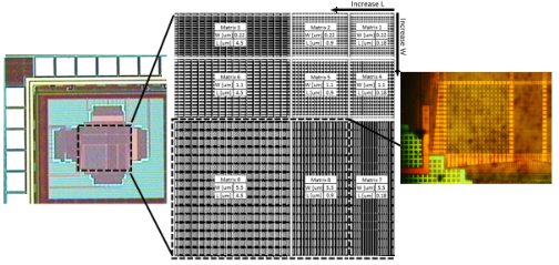
Fig: (a) Full circuit micrograph (b) MOSFET Matrix structure (c) Zoomed-in view at DUTs 

Acknowledgment: The authors would like to thank and acknowledge the Brazilian public company CEITEC S.A. Semiconductors for the measurement infrastructure, the CAD Support Center (NSCAD) at Federal University of Rio Grande do Sul (UFRGS) for electronic design automation (EDA) support, and Silterra Inc. for the silicon prototyping services.

Nov 3, 2020

ASCENT project

Applications and Systems-driven Center for Energy-Efficient integrated Nano Technologies

The Mission of the ASCENT Center is to transcend the current limitations of high-performance transistors confined to a single planar layer of integrated circuit by pioneering vertical monolithic integration of multiple interleaved layers of logic and memory, by demonstrating beyond-CMOS device concepts that combine processing and memory functions, heterogeneously integrating functionally diverse nano-components into integrated microsystems and by demonstrating in-memory compute kernels to accelerate future data-intensive at-scale cognitive workloads.

Researchers at ASCENT pursue four areas of technology including three-dimensional integration of device technologies beyond a single planar layer (vertical CMOS); spin-based device concepts that combine processing and memory functions (beyond CMOS); heterogeneous integration of functionally diverse nano-components into integrated microsystems (heterogeneous integration fabric); and hardware accelerators for data intensive cognitive workloads (merged logic-memory fabric).

ASCENT is one of six research centers funded by the SRC’s Joint University Microelectronics Program (JUMP), which represents a consortium of industrial participants and the Defense Advanced Research Projects Agency (DARPA). Information about the SRC can be found at https://www.src.org/.

Src Jump Logo

ASCENT is a collaboration of the following Universities:

Logo Cornell

Logo Georgia Tech
Logo ND

Logo Purdue

Logo Stanford

Logo Colorado
Logo Minnesota

Logo Berkeley

Logo UC San Diego

Logo UC Santa Barbara

Logo UCLA Logo UT Dallas

Logo Wayne Logo Illinois Institute


Congratulations to Prof. Robert W. Dutton

The 2020 IEEE EDS Celebrated Member and Esteemed EDS Alumni


Dr. Dutton received his degrees from the University of California, Berkeley, and currently instructs electrical engineering at Stanford University. Current members of EDS take pride in the Celebrated Members' accomplishments, drawing from their achievements as inspiration to advance and achieve success in various fields. The award presentation will be held virtually during the 2020 IEDM in December [read more...]

ROBERT W. DUTTON
Robert W. Dutton received the B.S., M.S., and Ph.D. in Electrical Engineering degrees from the University of California, Berkeley, in 1966, 1967, and 1970, respectively. 
He is currently Robert and Barbara Kleist Professor of Electrical Engineering at Stanford University, and Associate Chair for Undergraduate Education. He has held summer staff positions at Fairchild, Bell Telephone Laboratories, Hewlett‐Packard, IBM Research, and Matsushita during 1967, 1973, 1975, 1977, and 1988 respectively. His research interests focus on integrated circuit process, device, and circuit technologies, especially the use of computer‐aided design (CAD) and parallel computational methods. He has published more than 200 journal articles and graduated more than four dozen doctorate students. 
Dr. Dutton was Editor of the IEEE Transactions on Computer Aided Design from 1984 to 1986, the winner of the 1987 IEEE J. J. Ebers Award, 1988 Guggenheim Fellowship to study in Japan, elected to the National Academy of Engineering in 1991, 1996 Jack A. Morton Award, 2000 C&C Prize Japan, University Researcher Award, Semiconductor Industry Association (2000), Phil Kaufman Award, Electronic Design Automation Consortium (2006), and 2014 Bass University Fellow in Undergraduate Education Program, Stanford University.

Nov 2, 2020

Remember when the keyboard was the computer?

and in less than four (4) decades we are back: 

FROM Oric1:
a CPU (MOS 6502A @ 1 MHz) with 16KB ROM/48KB, Sound: AY-3-8912, Graphics: 40×28 text characters/ 240×200 pixels, 8 colours and simple connectivity - tape recorder I/O, Centronics compatible printer port, RGB video out, RF out, expansion port
TO Pi400:
a quad-core 64-bit @ 1.8GHz CPU Cortex-A72 (ARM v8) 64-bit (BCM2711) with 4GB RAM (LPDDR4-3200), wireless networking (IEEE 802.11b/g/n/ac wireless LAN, Bluetooth 5.0, BLE), dual-display output and 4K video playback it is ideal for surfing the web, creating and editing documents, watching videos, and learning to program using the Raspberry Pi
[read more: ]

[paper] SPICE Compact Model for Schottky-Barrier FETs

Sheikh Aamir Ahsan, Member, IEEE, Shivendra Kumar Singh, Chandan Yadav, Member, IEEE, Enrique G. Marín, Member, IEEE, Alexander Kloes, Senior Member, IEEE
and Mike Schwarz, Senior Member, IEEE
A Comprehensive Physics-Based Current–Voltage SPICE Compact Model 
for 2-D-Material-Based Top-Contact Bottom-Gated Schottky-Barrier FETs
IEEE Transactions on Electron Devices, vol. 67, no. 11, pp. 5188-5195, Nov. 2020
DOI: 10.1109/TED.2020.3020900

Abstract: In this article, we report the development of a novel physics-based analytical model for explaining the current–voltage relationship in Schottky barrier (SB) 2D material field effect transistors (FETs). The model has at its core the calculation of the surface-potential (SP) which is accomplished by invoking 2-D density of states in conjunction with Fermi–Dirac (FD) distribution for electron and hole statistics. The explicit computation for the SP, carried out using the Lambert-W function together with Halley’s method, is used to construct the SP-based band-diagram for realizing the transparency of the SBs. Thereafter, the ambipolar current is derived in terms of the electron and hole injection phenomena the thermionic emission and Fowler–Nordheim tunneling mechanisms at the SB contacts. Furthermore, drift-diffusion current is derived in terms of the SP and incorporated in the model to account for the scattering in the intrinsic 2D channel. Finally, the Verilog-A model is validated against experimental IV data reported in the literature for two different 2D material systems. This is the first demonstration of an explicit SP-based SPICE model for ambipolar SB-2-D-FETs that is simultaneously built on tunneling-emission and driftdiffusion formalisms.

Fig: (a) Band-diagram sketched along positive y-direction underneath the source electrode. Blue and black lines represent bands before and after applying Vgs. (b) ψ-based diagram sketched along positive x, constructed after calculating ψs and ψd. The geometrical screening length λ is given by λ ≈ (tox t2D)^1/2.

Acknowledgement: This work was supported in part by the National Project Implementation Unit (NPIU) through the third phase of Technical Education Quality Improvement Programme (TEQIP-III) Project and in part by DST-SERB Startup Research Grant under Award SRG/2019/001122.


[paper] Process Induced Vt Variability

Mandar S. Bhoir, Member, IEEE, Thomas Chiarella, Jerome Mitard, Naoto Horiguchi, Member, IEEE, and Nihar Ranjan Mohapatra, Senior Member, IEEE
Vt Extraction Methodologies Influence Process Induced Vt Variability:
Does This Fact Still Hold for Advanced Technology Nodes? 
IEEE Transactions on Electron Devices, vol. 67, no. 11, pp. 4691-4695, Nov. 2020
DOI: 10.1109/TED.2020.3025750.

Abstract: In this work, we have investigated the influence of Vt extraction procedure on overall Vt variability of sub-10 nm Wfin FinFETs. Using six different Vt extraction techniques (These are 1) constant current (CC) technique, 2) extrapolation in linear regime [ELR, also known as maximum trans-conductance (gm)] technique, 3) trans-conductance extrapolation (TCE) technique, 4) second-derivative (SD) technique, 5) ratio method (RM); and 6) transition method (TM) [1]) we have experimentally demonstrated that the Vt variability is independent of Vt extraction procedure (unlike reported earlier). Furthermore, through systematic evaluation on commonly used Vt extraction techniques, the physics behind this anomalous behavior is investigated. It is shown that the significant variation in metal gate work-function and gate dielectric charges in advanced CMOS nodes is mainly responsible for this behavior. This claim is further validated for FinFETs with deeply scaled fin-width and effective oxide thickness (EOT).


Fig: (a) Schematic illustration of different process-variability sources in FinFET; 
(b)Transfer characteristics for FinFETs with similar Vt, CC but different RSD.
These FinFETs have different Vt, ELR because of RSD induced gm, max variations

Acknowleegement: This work was supported in part by the Visvesvaraya Ph.D. Scheme, MeitY, Government of India MEITY-PHD-250 and in part by the Horizon 2020 ASCENT EU Project (Access to European Nanoelectronics Network) under Project 654384.

References:
[1] A. Ortiz-Conde, F. G. Sánche, J. J. Liou, A. Cerdeira, M. Estrada, and Y. Yue, “A review of recent MOSFET threshold voltage extraction methods,” Microelectron. Rel., vol. 42, no. 4, pp. 583—596, 2002, doi: 10.1016/S0026-2714(02)00027-6

Engineers at #PSU have demonstrated an #analog non-volatile #memory that can operate as a close mimic of the #synapse within the brain. https://t.co/fpykOONXAf #semi https://t.co/eHbD4Uez0a


from Twitter https://twitter.com/wladek60

November 02, 2020 at 01:50PM
via IFTTT

#TSMC to Build Fab in #Arizona and They are #Hiring! https://t.co/AtMOY6j3ox #semi https://t.co/zfWFCKx3JT


from Twitter https://twitter.com/wladek60

November 02, 2020 at 11:22AM
via IFTTT

Oct 30, 2020

Video Tutorial: What is Verilog-A

Video Tutorial: What is Verilog-A

Verilog-A is a behavioural modelling language for analog circuits from the Verilog Family. It is the subset of Verilog-AMS. Verilog-A HDL is derived from the IEEE 1364 Verilog HDL specification. The intent of Verilog-A HDL is to let designers of analog systems and integrated circuits create and use modules that encapsulate high-level behavioural descriptions as well as structural descriptions of systems and components.

Reference: 
[1] OVI Verilog-A LRM , 1996
[2] https://literature.cdn.keysight.com/litweb/pdf/ads2004a/pdf/verilogaref.pdf
[3] A New Approach to Compact Semiconductor device Modelling with Qucs Verilog-A analog module synthesis, M.E Brinson & V Kuznetsov, International Journal of Numnerical Mdelling, 2015
[4] https://github.com/cogenda/VA-BSIM48/blob/master/bsim4_release.va

[PhD Thesis] III-V MOS-HEMTs for 100-340GHz Communications Systems

UNIVERSITY OF CALIFORNIA
Santa Barbara
III-V InxGa1-xAs / InP MOS-HEMTs for 100-340GHz Communications Systems
A dissertation for PhD degree in Electrical and Computer Engineering
by Brian David Markman

Abstract: This work summarizes the efforts made to extend the current gain cutoff frequency of InP based FET technologies beyond 1THz. Incorporation of a metal-oxide-semiconductor field effect transistor (MOSFET) at the intrinsic Gate Insulator-Channel interface of a standard high electron mobility transistor (HEMT) has enabled increased gm,i by increasing the gate insulator capacitance density for a given gate current leakage density. Reduction of RS,TLM from 110 Ω.μm to 75Ω.μm and Ron(0) from 160Ω.μm to 120Ω.μm was achieved by removing/thinning the wide bandgap modulation doped link regions beneath the highly doped contact layers. Process repeatability was improved by developing a gate metal first process and Dit was improved by inclusion of a post-metal H2 anneal. InxGa1-xAs / InAs composite quantum wells clad with both InP and InxAl1-xAs were developed for high charge density and low sheet resistance to minimize source resistance. 
Figure a) InP-based HEMT b) III-V DC optimized MOSFET c) proposed InP-based MOS-HEMT

[Citation] Markman, B. D. (2020). III-V InxGa1-xAs / InP MOS-HEMTs for 100-340GHz Communications Systems. UC Santa Barbara. ProQuest ID: Markman_ucsb_0035D_14853. Merritt ID: ark:/13030/m5v4681j. Retrieved from https://escholarship.org/uc/item/6st812pb

Oct 29, 2020

#Congratulations to Dr. Arokia Nathan J.J. Ebers Award winner


from Twitter https://twitter.com/wladek60

October 29, 2020 at 08:49AM
via IFTTT

Fwd: Patrick Fay DL - III-N Nanowire FETs for Low-Power Applications

Patrick Fay DL - III-N Nanowire FETs for Low-Power Application

The EDS Germany Chapter and NanoP proudly presents Patrick Fay from University of Notre Dame, Indiana, USA
for a Distinguished Lecture on "III-N Nanowire FETs for Low-Power Applications". The lecture will be held on
23th November 2020 at 3pm Berlin time.  To view complete details for this event, click here to view the announcement

Date and Time

Location

The Distiguished Lecture will be held via Zoom. Login information provided before the event and requires registration.

  • Virtual
  • Germany
Staticmap?size=250x200&sensor=false&zoom=14&markers=51.53771465%2c7

Hosts

Registration <https://events.vtools.ieee.org/m/245747>

  • Starts 29 October 2020 08:00 AM
  • Ends 21 November 2020 12:00 AM
  • All times are Europe/Berlin
  • No Admission Charge

Oct 28, 2020

EDTM 2021, Chengdu (CN): March 9-12, 2021

EDTM Conference 2021, Chengdu, China, between March 9th to 12th, 2021
Paper Submission Deadline: November 7 2020


IEEE LOGOEDS LOGO

EDTM2021 LOGO

The IEEE Electron Devices Technology and Manufacturing (EDTM) Conference 2021 is a four-day meeting to be held in Chengdu, China, during March 9th to 12th, 2021. Sponsored by IEEE Electron Devices Society (EDS), EDTM2021 is a premier conference, providing a unique forum for discussions on a broad range of device/manufacturing-related topics. EDTM2021 starts on Tuesday, March 9, 2021 with Tutorial & Short Courses, followed by three days of Plenary talks and parallel Oral sessions. Joint Poster sessions and Exhibition will be held on the same site.

EDTM2021 Theme: Intelligent Technologies for Smart and Connected Life.

CHENGDU PHOTO

▪ Technical Areas

EDTM2021 solicits papers in all areas of electron devices, including materials, processes, devices, packaging, modeling, reliability, manufacturing and yield, tools, testing, and any emerging device technologies.

EDTM2021 cordially invites authors to submit your papers.

Please refer to the EDTM2021 website for more details, or clink links below:

EDTM2021 website: https://ewh.ieee.org/conf/edtm/2021/

Call for Papers

▪ Sponsorship & Exhibition

EDTM2021 also warmly invites sponsors and exhibitors to participate in and support the conference where you can showcase your new technologies and products to attendees from around the world.

Call for Sponsorship

Call for Exhibitors

▪ Awards

EDTM2021 will select Best Paper Award, Best Student Paper Award and Best Poster Paper Award.

▪ Publications

All selected and presented papers will be included in the EDTM2021 Proceedings that will be published at the IEEE Xplore. Selected papers will be invited to submit the extended manuscripts that will be reviewed for possible publication in the IEEE Journals of Electron Devices Society (J-EDS), which is an Open Access journal.

▪ Important Dates

Paper Submission Starts

August 1, 2020

Paper Submission Deadline

November 7 2020  

Notification of Acceptance

December 20, 2020

EDTM2021 Conference

March 9 - 12, 2021

▪ Location

Chengdu, located in southwest of China, is not just the home for Grand Pandas. An emerging technology and business hub full of hi-tech companies from around the world, it is also a trendy city where you will find everything that you could imagine for you to enjoy your leisure time, from the famous Sichuan food to mind-soothing teas to natural scenics to historical wonders. The wonderful city is just an easy flight away from many places around the Globe.

▪ Contacts

General Chair:
Albert Wang, University of California, Riverside,
aw@ece.ucr.edu

General Co-Chair:
Tianchun Ye, IME-CAS,
tcye@ime.ac.cn

TPC Chair:
Huaqiang Wu, Tsinghua University,
wuhq@tsinghua.edu.cn

TPC Co-Chair:
Subramanian Iyer, University of California, Los Angeles,
s.s.iyer@ucla.edu

COVID-19 Watch: Chengdu remains safe. EDTM2021 is planned as an in-person/on-site event. Meanwhile, we are closely monitoring the development of global COVID-19 outbreak. A contingency plan will allow virtual presentations and participation for those with travel restrictions and concerns. Both safety and participation experiences will be ensured for EDTM2021.

PANDA PHOTO

EDTM2021 website: https://ewh.ieee.org/conf/edtm/2021/


The Future of CERN’s Large Hadron Collider For Humanity a Necessity or a Waste? https://t.co/xzCoofmtBN #semi https://t.co/O7vWjmFloj


from Twitter https://twitter.com/wladek60

October 28, 2020 at 11:03AM
via IFTTT

Prof. Michael Shur: IEEE EDS DL - Counter Intuitive Physics of Ballistic Transport in the State-of-the-Art Electronic Devices


The EDS Germany Chapter and NanoP proudly presents Michael Shur from Rennselaer Polytechnic Institute, New York, USA for a Distinguished Lecture on "Counter Intuitive Physics of Ballistic Transport in the State-of-the-Art Electronic Devices"

Date and Time

Location

The Distiguished Lecture will be held via Zoom. Login information provided before the event and requires registration.

  • Virtual
  • Germany

Hosts

Registration

  • Starts 28 October 2020 07:00 AM
  • Ends 14 November 2020 12:00 AM
  • All times are Europe/Berlin
  • No Admission Charge

Oct 27, 2020

[paper] Optomechanical Sensor in Verilog-A

Houssein Elmi Dawale, Loïc Sibeud, Sébastien Regord, Guillaume Jourdan, Member, IEEE, Sébastien Hentz, Member, IEEE, and Franck Badets, Senior Member, IEEE
Compact Modeling and Behavioral Simulation of an Optomechanical Sensor in Verilog-A
IEEE Transactions on Electron Devices, vol. 67, no. 11, pp. 4677-4681, Nov. 2020
DOI: 10.1109/TED.2020.3024477

Abstract: Previous work has shown that optomechanical resonators are particularly well suited to the design of ultrasensitive mass sensors. They present an extremely low noise level, very high optical quality factor (Q>105), excellent integration density and can resonate both in a gaseous and liquid environment. In order to reduce the long measurement time due to their small particle capture area, several such resonators must be integrated onto the same chip. However, bulky laboratory equipment currently used to read a single optomechanical resonator cannot be practically scaled up to a large array of transducers. It is then required to design and eventually integrate a read-out interface that can process tens to thousands of resonators. To ease the design of such a circuit, this article presents a compact analytical model of an electrostatically actuated optomechanical resonator implemented in Verilog-A. The proposed model includes both the optical and mechanical behaviors, as well as optomechanical coupling and thermo-optical effect. It was simulated in commercial simulator and is consistent with the measured results. 
FIG: a) General view of the optomechanical device with electrostatic actuation. 
b) Functional diagram of the device in Verilog-A.


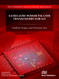
[book] Ultra-Low Power FM-UWB Transceivers for IoT

book cover image
Ultra-Low Power FM-UWB Transceivers for IoT
Vladimir Kopta and Christian Enz
River Publishers, 2020, pp.i-xxiv

Over the past two decades we have witnessed the increasing popularity of the internet of things. The vision of billions of connected objects, able to interact with their environment, is the key driver directing the development of future communication devices. Today, power consumption as well as the cost and size of radios remain some of the key obstacles towards fulfilling this vision. Ultra-Low Power FM-UWB Transceivers for IoT presents the latest developments in the field of low power wireless communication. It promotes the FM-UWB modulation scheme as a candidate for short range communication in different IoT scenarios. The FM-UWB has the potential to provide exactly what is missing today. This spread spectrum technique enables significant reduction in transceiver complexity, making it smaller, cheaper and more energy efficient than most alternative options. The book provides an overview of both circuit-level and architectural techniques used in low power radio design, with a comprehensive study of state-of-the-art examples. It summarizes key theoretical aspects of FM-UWB with a glimpse at potential future research directions. Finally, it gives an insight into a full FM-UWB transceiver design, from system level specifications down to transistor level design, demonstrating the modern power reduction circuit techniques. Ultra-Low Power FM-UWB Transceivers for IoT is a perfect text and reference for engineers working in RF IC design and wireless communication, as well as academic staff and graduate students engaged in low power communication systems research.

[paper] Wearable Circuits for Health Monitoring

Ling Zhang, †,‡,§ Hongjun Ji, †,‡,# Houbing Huang, ^ Ning Yi, ǂ,& Xiaoming Shi, ^ Senpei Xie, ‡,# Yaoyin Li, ‡,# Ziheng Ye, # Pengdong Feng, ‡,# Tiesong Lin, † Xiangli Liu, # Xuesong Leng, † Mingyu Li, †,‡,# Jiaheng Zhang, †,‡,# Xing Ma, †,‡,# Peng He, † Weiwei Zhao, †,‡,#
and Huanyu Cheng, §,ǂ
Wearable Circuits Sintered at Room Temperature Directly on The Skin Surface for Health Monitoring
ACS Appl. Mater. Interfaces 2020, 12, 40, 45504–45515
Publication Date:September 11, 2020
DOI: 10.1021/acsami.0c11479

†State Key Laboratory of Advanced Welding & Joining, Harbin Institute of Technology, Shenzhen, 518055, People’s Republic of China
‡Flexible Printed Electronics Technology Center, Harbin Institute of Technology, Shenzhen, 518055, People’s Republic of China
§Department of Engineering Science and Mechanics, The Pennsylvania State University, University Park, PA 16802, USA.
#The School of Material Science and Engineering, Harbin Institute of Technology, Shenzhen, 518055, People’s Republic of China
^Advanced Research Institute of Multidisciplinary Science, Beijing Institute of Technology, Beijing 100081, China
ǂDepartment of Materials Science and Engineering, The Pennsylvania State University, University Park, PA 16802, USA.

Abstract: A soft body area sensor network presents a promising direction in wearable devices to integrate on-body sensors for physiological signal monitoring and flexible printed circuit boards (FPCBs) for signal conditioning/readout and wireless transmission. However, its realization currently relies on various sophisticated fabrication approaches such as lithography or direct printing on a carrier substrate before attaching to the body. Here we report a universal fabrication scheme to enable printing and room-temperature sintering of metal nanoparticle on paper/fabric for FPCBs and directly on the human skin for on-body sensors with a novel sintering aid layer. Consisting of polyvinyl alcohol (PVA) paste and nanoadditives in the water, the sintering aid layer reduces the sintering temperature. Together with the significantly decreased surface roughness, it allows for the integration of a submicron-thick conductive pattern with enhanced electromechanical performance. Various on-body sensors integrated with an FPCB to detect health conditions illustrate a system-level example.
Fig: Print These Electronic Circuits Directly Onto Skin by spectrum.ieee.org

Acknowledgment: This work was supported by several grants provided by The Pennsylvania State University and National Science Foundation (NSF) (Grant No. ECCS-1933072) to H.C., as well as Shenzhen Science and Technology Program (Grant No. KQTD 20170809110344233, JCYJ 20170811160129498) and Bureau of Industry and Information Technology of Shenzhen through the Graphene Manufacturing Innovation Center (201901161514). X.L. acknowledges the support from the Natural Science Foundation of China (11672090)

[Open PhD] IMEC: Modeling of hybrid nanofluidic-nanoelectronic devices for single-molecule biosensing


from Twitter https://twitter.com/wladek60

October 27, 2020 at 09:15AM
via IFTTT

Fwd: IEEE-EDS Santa Clara Valley/San Francisco Chapter October Seminar (Webex only)

Please note that this seminar is now WEBEX participation only. 

Coupled Oscillator based Computing: Using Nature to Solve Difficult Problems
Prof. Chris H. Kim, University of Minnesota
Friday, October 30, 2020 at 11AM – noon PDT


Abstract:
In this talk, I will introduce a first-of-its kind quantum-inspired coupled oscillator based compute engine implemented in a standard 65nm technology targeted for NP-hard or NP-complete problems such as max-cut, graph coloring, traveling salesman, and pattern recognition. The NP-hard problem is first mapped to the coupling weights while the solution is represented by the phases of the individual oscillators, which are read out using on-chip phase sampling circuits. Our hardware exploits the natural tendency of a network of coupled oscillator to settle to the ground state, which offers significant performance and power advantages compared to traditional digital approaches.

Speaker Bio:
Chris H. Kim received his B.S. and M.S. degrees from Seoul National University and a Ph.D. degree from Purdue University. He is currently a professor at the University of Minnesota. Prof. Kim is the recipient of the University of Minnesota Taylor Award for Distinguished Research, SRC Technical Excellence Award, Council of Graduate Students Outstanding Faculty Award, NSF CAREER Award, Mcknight Foundation Land-Grant Professorship, 3M Non-Tenured Faculty Award, DAC/ISSCC Student Design Contest Award, IBM Faculty Partnership Award, IEEE Circuits and Systems Society Outstanding Young Author Award, the ICCAD Ten Year Retrospective Most Influential Paper Award, ISLPED Low Power Design Contest Award (4 times), and ISLPED Best Paper Award (2 times). His group has expertise in digital, mixed-signal, and memory IC design, with special emphasis on circuit reliability, hardware security, memory circuits, radiation effects, time-based circuits, beyond-CMOS technologies, and machine learning hardware design. He is an IEEE fellow.


Subscribe or Invite your friends to sign up for our mailing list and get to hear about exciting electron-device relevant talks. We promise no spam and try to minimize email. http://site.ieee.org/scv-eds/subscribe/

Oct 26, 2020

[paper] 2D-SFET Based SRAMs

Niharika Thakuria, Graduate Student Member, IEEE, Daniel Schulman, Member, IEEE, Saptarshi Das, Member, IEEE, and Sumeet Kumar Gupta, Member, IEEE
2D Strain FET (2D-SFET) Based SRAMs - Part I: Device-Circuit Interactions
 IEEE TED, vol. 67, no. 11, pp. 4866-4874, Nov. 2020
DOI: 10.1109/TED.2020.3022344.

Abstrat: In this article, we analyze the characteristics of a recently conceived steep switching device 2-D Strain FET (2D-SFET) and present its circuit implications in the context of 6T-SRAM. We discuss the dependence of 2D-SFET characteristics on key design parameters, showing up to 2.7× larger ON-current and 35% decrease in subthreshold swing when compared to 2D-FET. We analyze the performance of 2D-SFET (as drop-in replacement for standard 2D-FET) in 6T-SRAM for a range of design parameters and compare those to 2D-FET 6T-SRAM. 2D-SFET 6T-SRAM achieves up to 5.7% lower access time, 63% higher write margin, and comparable hold margin, but at the cost of comparable to 11% lower read stability and 16% increase in write time. In Part II of this article, we mitigate the read stability issues of 2D-SFET SRAMs by proposing VB-enabled SRAM designs.
Fig: 2D-SFET model with bandgap reduction and 2-D-electrostatics [18]. COX, CGS/D,F, CIT, and CGB are oxide, gate (G) to source (S)/drain (D) fringe, trap, and PE capacitance, respectively. VFB, and VFBS are flat-band voltage of G and back contact. VQFL(VS,VD) is S/D quasiFermi level. ΔEG(VG'B) is VGB dependent bandgap change, τEG is strain transduction delay, and REG is resistance used to model τEG. ΔEG(τEG) is final bandgap reduction considering τEG, used for calculating channel charge, QCH(ΔEG(τEG)).

Aknowlegement: This work was supported in part by NSF under Grant 1640020, in part by Nanoelectronics Research Corporation (NERC), and in part by Semiconductor Research Corporation (SRC) under Grant 2699.003

[CAS Seasonal School] How Technology is Impacting Agribusiness

How Technology is Impacting Agribusiness

A CAS seasonal school on technology and agribusiness will be held virtually from November 16th to November 20th. The program is quite interesting and we invite you to register through our web page www.asic-chile.cl. Registration is free.

The current world population of 7.6 billion is expected to reach 9.8 billion in 2050. According to the United Nations Food and Agriculture Organization (FAO) global agricultural productivity must increase by 50% – 70% to be able to feed the world population in 2050. Other researchers consider that reducing the waste of food would be enough.

Factors if not obstacles to be considered to meet global food demand by 2050 and beyond:
  • Less arable land: As cities are growing, the space allowed to agriculture is shrinking.
  • Climate change: Impacting dramatically agribusiness.
  • Role of the agribusiness on the GHG emissions.
  • Planet boundaries and the role of agribusiness.
  • Availability of freshwater.
  • Soil degradation.
The need has never been greater for innovative and sustainable solutions and technology should lead to significant improvement in our food and nutritional security.

In this seasonal school prestigious researchers and experts from all over the world will present the problems and challenges agribusiness is facing and how technologies such as IoT, AI, Machine Learning, sensors, electronic circuits, electronic systems, ICs, etc., can be applied to improve and solve the majority of those problems.

This is the first of a series of “Technology and Agribusiness” Seasonal Schools. It will be a meeting point for professionals working on Precision and Smart Agriculture, as well as professionals working on IoT, sensors, electronic circuits, electronic systems, ICs, etc.

We invite you to participate in this first version of the Technology and Agribusiness Seasonal School, which due to the pandemic will be 100% online and free of charge.

Join us!

[paper] Organic semiconductor (OSC) OFETs

Boyu Peng, Ke Cao* Albert Ho Yuen Lau, Ming Chen, Yang Lu* and Paddy K. L. Chan
Crystallized Monolayer Semiconductor for Ohmic Contact Resistance, High Intrinsic Gain, and High Current Density
Adv. Mater. 2020, 32, 2002281 
DOI:10.1002/adma.202002281

Department of Mechanical Engineering, The University of Hong Kong, Pokfulam Road (HK)
*Department of Mechanical Engineering, City University of Hong Kong, Kowloon (HK)

Abstract: The contact resistance limits the downscaling and operating range of organic field-effect transistors (OFETs). Access resistance through multilayers of molecules and the nonideal metal/semiconductor interface are two major bottlenecks preventing the lowering of the contact resistance. In this work, monolayer (1L) organic crystals and nondestructive electrodes are utilized to overcome the abovementioned challenges. High intrinsic mobility of 12.5 cm2 V−1 s−1 and Ohmic contact resistance of 40 Ω cm are achieved. Unlike the thermionic emission in common Schottky contacts, the carriers are pre- dominantly injected by field emission. The 1L-OFETs can operate linearly from VDS = −1 V to VDS as small as −0.1 mV. Thanks to the good pinch-off behavior brought by the monolayer semiconductor, the 1L-OFETs show high intrinsic gain at the saturation regime. At a high bias load, a maximum current density of 4.2 µA µm−1 is achieved by the only molecular layer as the active channel, with a current saturation effect being observed. In addition to the low contact resistance and high-resolution lithography, it is suggested that the thermal management of high-mobility OFETs will be the next major challenge in achieving high-speed densely integrated flexible electronics.

Fig: a) Schematic charge accumulation and b) output curves of short-channel OFETs. c) Schematic charge accumulation and d) output curves of source-gated transistors. e) Schematic charge accumulation and f) output curves of 1L-OFETs. 

Acknowledgements: The authors gratefully acknowledge the support from the General Research Fund (GRF) under Grant Nos. HKU 17264016 and HKU 17204517, University of Hong Kong Seed Funding Grant Nos. 201711159068 and 201611159208. The authors appreciate Prof. Xin Cheng and Xin Zhuang from Southern University of Science and Technology for their support on e-beam lithography. The authors also thank Dr. Hagen Klauk and James W. Borchert for the fruitful discussions and suggestions.

Oct 25, 2020

[paper] Compact Modeling of Organic TFT

Jakob Pruefer, Jakob Leise, Ghader Darbandy, Aristeidis Nikolaou, Hagen Klauk, James W. Borchert, Benjamín Iñíguez, Fellow, IEEE, Thomas Gneiting, Member, IEEE
and Alexander Kloes, Senior Member, IEEE
Compact Modeling of Short-Channel Effects in Staggered Organic Thin-Film Transistors
IEEE Transactions on Electron Devices, vol. 67, no. 11, pp. 5082-5090, Nov. 2020
DOI: 10.1109/TED.2020.3021368.

Abstract:This article introduces analytical compact models of short-channel effects in staggered organic thinfilm transistors (TFTs). The effects of subthreshold-swing degradation, threshold-voltage roll-off, and drain-induced barrier lowering (DIBL) on the static current–voltage characteristics of staggered TFTs are extracted from an analytical potential solution of the 2-D problem of the staggered geometry. This solution is derived by using the Schwarz–Christoffel transformation that leads to a complex mapping function linking the staggered geometry to an equivalent in another coordinate system for which an analytical potential solution exists. The commercial TCAD is used to verify the compact models. Finally, the closed-form and physics-based equations are incorporated into an existing compact current model and verified by measurements on staggered organic TFTs with channel lengths as small as 0.4 µm fabricated on flexible plastic substrates by stencil lithography.
Fig:(a) Schematic cross section and (b) simplified geometry 
of the staggered organic TFTs for the TCAD simulations.

Acknowledgement: This work was supported in part by the German Federal Ministry of Education and Research under Grant 13FH015IX6 Strukturnahe Modellierung organischer flexibler KurzkanalTFTs (Structure-Oriented Modeling of Organic FLEXible short-channel TFTs) (SOMOFLEX), in part by the EU H2020 Marie Sklodowska-Curie actions (MSCA) Research and Innovation Staff Exchange (RISE) Project Design Oriented ModellINg for flexible electrOnics (DOMINO) under Grant 645760, and in part by the German Research Foundation (DFG) under Grant KL 1042/9-2 (SPP FFlexCom). 

Oct 23, 2020

[paper] Capacitive Sensor for Dental Implants

Alireza Hassanzadeh, Ali Moulavi and Amir Panahi
A New Capacitive Sensor for Histomorphometry Evaluation of Dental Implants
in IEEE Sensors Journal, 
DOI: 10.1109/JSEN.2020.3026745

Abstract: Knowing information about the internal functions of the human body has always been the subject of scientific research. Processing of the data from inside of the body gives access to valuable information for the therapist. In this paper, an implantable capacitive sensor has been designed and implemented inside the bone to evaluate the new bone growth. Reducing the medical x-ray imaging dose during a jaw scan is a motivation for the design of the sensor. The new capacitive sensor can replace multiple x-ray imaging sessions. Low energy consumption, stable performance, and information processing rate are some of the engineering challenges for implanted sensors. The designed sensor is a zero power module, which can easily be implemented in dental tooth implants without any active component. The capacitive sensor information can be transmitted to a reader device via a wireless inductive link. The sensor simulation results from a commercial software confirm experimental measurements. The fabricated sensor has been tested on the femur (thigh) bone and mandible bone (lower jaw). The sensor capacitance changes from 20nF to 1.57μF for the fabricated sensor and amount of the surrounding bone. Fabrication results show that variation of sensor capacitance from the early stage of the dental implant to full recovery and bone development is more than seven times. The wide range of sensor capacitance variation allows for better bone development characterization. 

Fig: a) Schematic of a typical sensor and reader inductive link, b) Reader and the implanted sensor.

[report] OptiBP smartphone app

Patrick Schoettker1, Jean Degott1, Gregory Hofmann1, Martin Proença2, Guillaume Bonnier2, Alia Lemkaddem2, Mathieu Lemay2, Raoul Schorer3, Urvan Christen4, Jean‑François Knebel4, Arlene Wuerzner5, Michel Burnier5 and Gregoire Wuerzner5 
Blood pressure measurements with the OptiBP smartphone app validated against reference auscultatory measurements
Scientific Reports Vol. 10, Article number: 17827 (2020)
DOI: 10.1038/s41598-020-74955-4 
  
1Department of Anesthesiology, Lausanne University Hospital and University of Lausanne (CH)
2CSEM, Swiss Center for Electronics and Microtechnology, Neuchâtel (CH)
3Department of Acute Medicine, Geneva University Hospital and University of Geneva, (CH)
4Biospectal SA, 1003 Lausanne (CH)
5Service of Nephrology and Hypertension, Lausanne University Hospital and University of Lausanne,  (CH)

Abstract: Mobile health diagnostics have been shown to be efective and scalable for chronic disease detection and management. By maximizing the smartphones’ optics and computational power, they could allow assessment of physiological information from the morphology of pulse waves and thus estimate cufess blood pressure (BP). We trained the parameters of an existing pulse wave analysis algorithm (oBPM), previously validated in anaesthesia on pulse oximeter signals, by collecting optical signals from 51 patients fngertips via a smartphone while simultaneously acquiring BP measurements through an arterial catheter. We then compared smartphone-based measurements obtained on 50 participants in an ambulatory setting via the OptiBP app against simultaneously acquired auscultatory systolic blood pressure (SBP), diastolic blood pressure (DBP) and mean blood pressure (MBP) measurements. Patients were normotensive (70.0% for SBP versus 61.4% for DBP), hypertensive (17.1% vs. 13.6%) or hypotensive (12.9% vs. 25.0%). The diference in BP (mean± standard deviation) between both methods were within the ISO 81,060–2:2018 standard for SBP (− 0.7 ± 7.7 mmHg), DBP (− 0.4 ± 4.5 mmHg) and MBP (− 0.6 ± 5.2 mmHg). These results demonstrate that BP can be measured with accuracy at the fnger using the OptiBP smartphone app. This may become an important tool to detect hypertension in various settings, for example in low-income countries, where the availability of smartphones is high but access to health care is low. 
Fig: OptiBP application utilizes image data generated from volumetric blood fow changes via light passing through the fngertip, refecting of of the tissue, and then passing to the phone camera’s image sensor.

Acknowledgements: We thank Dr. Frederic Michard from MiCo (michardconsulting.com) for help in manuscript preparation. With funding of Innosuisse—Swiss Innovation Agency, Project no. 32688.1 IP-ICT.

Oct 21, 2020

[Survey] Power Amplifiers Performance 2000-Present

Fifth web release on 2020/10/15: "PA_Survey_v5". This version-5 dataset includes PAs/transmitters from 500MHz to 1.5 THz in Bulk/SOI CMOS, SiGe, LDMOS, InP, GaN, GaAs technologies. The dataset contains total 3207 data points with over 1200 data points for CMOS, SiGe PAs and over 1500 data points for GaN, GaAs, InP PAs.

We have added sub-THz/THz power/signal generation circuits from 15GHz to 1.5THz, including PAs, fundamenal/harmonic oscillators, and frequency multipliers, to support the emerging research on beyond-5G/6G applications.

The file "PA_Survey_v5" is the version-5 dataset that includes ALL the reported PA/transmitter data since 2000 over frequency and various technologies. It also includes summary plots on CW Psat vs. Carrier Frequency for different technologies, peak PAE vs. CW Psat at different frequencies, and average PAE vs. average Pout for high-order complex modulations.

What is new in version-5 release beyond the version-4 release? 500MHz to 1.5 THz Power Amplifier designs and sub-THz/THz power/signal generation circuits published between 02/2020 and 10/2020.

  • Cite this PA survey: Hua Wang, Tzu-Yuan Huang, Naga Sasikanth Mannem, Jeongseok Lee, Edgar Garay, David Munzer, Edward Liu, Yuqi Liu, Bryan Lin, Mohamed Eleraky, Sensen Li, Fei Wang, Amr S. Ahmed, Christopher Snyder, Sanghoon Lee, Huy Thong Nguyen, and Michael Edward Duffy Smith, "Power Amplifiers Performance Survey 2000-Present," [Online]. Available: https://gems.ece.gatech.edu/PA_survey.html
  • Acknowledgement: We would like to sincerely thank many of our friends and colleagues for their helpful suggestions and insightful discussions.
  • Feedback and Suggestions: We welcome your feedback and suggestions, including the ways to interpret and present the data. In addition, although we try to be as inclusive as possible when collecting these published data, it is certainly possible that we may miss some representative PA designs. Please feel free to send us feedback, suggestions, or missing PA papers.
  • Contact: Please contact us through poweramplifiers.survey at gmail dot com. Do not use my gatech email address, since I may very likely miss your email.
  • Source for this data collection: We focus on peer-reviewed and publicly accessible publications that are typical forums for PAs, including IEEE ISSCC, JSSC, RFIC, VLSI, CICC, ESSCIRC, IMS, T-MTT, TCAS, BCTM/CSICS (BCICTS in the future), APMC, EuMC, and MWCL. We also focus on public product datasheets on PAs/transmitters.


Oct 20, 2020

[Open PhD] #IMEC


from Twitter https://twitter.com/wladek60

October 20, 2020 at 05:46PM
via IFTTT