Dec 5, 2014

Call for Papers PRIME 2015

 The PRIME 2015 Call for Papers is available at: 
 http://web.eng.gla.ac.uk/prime2015/static/images/PRIME2015CFPv2.pdf 

The purpose of the PRIME Conference is to grow Ph.D students' experience in the early stage of their career by creating a connection between academic world and companies.

A Workshop is organized for all conference participants on June 29th. Moreover, a Company Fair is organized for all conference participants, to create a connection between major companies in Electronics/Microelectronics and Ph. D students.

PRIME 2015 topics of interest include, but are not limited, to:

  • Micro/nanoelectronics
  • Semiconductors
  • Analog and Digital Signal Processing
  • Computer Aided Design
  • Analog, Digital, Mixed-Signal and RF IC Design
  • Integrated Power ICs
  • RF, Microwave and Millimeterwave Circuits
  • VLSI and SoC Applications
  • Visual Signal Processing
  • Sensor Systems and MEMS
  • Energy Scavenging
  • Technical trends and challenges
  • Electronic Skin

Dec 2, 2014

Meet with Silvaco at IEDM 2014

Silvaco will showcase at IEDM products for applications such as displays, power devices, optical devices, advanced CMOS process development, radiation & soft error reliability, analog and memory design.
  • Victory Process, Device and Stress for 1D, 2D and 3D TCAD simulation for applications such as TFT displays, IGBT power devices, lasers, image sensors, advanced CMOS devices such as FDSOI and FinFETs, radiation and soft error reliability simulation
  • Clever for 3D parasitic RC extraction with the highest accuracy capacitance extraction for application such as TFT design, FinFET SRAM analysis
  • Utmost IV for creating SPICE models for any device type including TFT, UOTFT, BSIM-CMG for FinFETs, HSIM-HV2 for high voltage devices
  • Affordable and complete custom design flow including schematic entry, layout, simulation, analysis and verification ideally suited to analog, power management applications and for process nodes such as 65nm/40nm that are key targets for Internet of Thing (IoT) designs
  • SmartSpice for simulation of circuits such as analog/mixed-signal, HSIO, RF, SRAM, standard cells, TFT panels, power ICs and for which recent performance enhancement benchmark data will be shared
  • SmartSpice for library, memory and critical path characterization with built-in optimizers and circuit rubber-banding capability, having achieved 16nm FinFET model certification and includes PODE and ETMI reliability model support
  • SmartSpice Soft Error Reliability capability that is used to analyze the impact of Single Event Effects (SEE) on circuit performance, an increasingly important challenge at 20nm and below technology nodes 
More information at their website.

Nov 20, 2014

[mos-ak] FOSDEM 2015 Electronic Design Automation Devroom Call for Participation

 This is the call for participation in the FOSDEM 2015 devroom on Free/Open Source Software (FOSS) Electronic Design Automation (EDA) tools, to be held on Sunday 1 February 2015 in Brussels, Belgium. We are looking for contributions under the form of talks covering the following main topics:
We hope to provide an opportunity for attendees to bring themselves up to date on the latest FOSS EDA developments, share knowledge and identify opportunities to collaborate on development tasks.

The submission process

Please submit your proposals at https://penta.fosdem.org/submission/FOSDEM15 before 1 December 2014.

If you already have a Pentabarf account (for example as a result of having submitted a proposal in the past), make sure you use it to log in and submit your proposal. Do not create a new account if you already have one. Please provide a bit of information about yourself in Person -> Biography. When you submit your proposal (creating an "Event" in Pentabarf), make sure you choose the "Electronic design automation devroom" in the track drop-down menu. Otherwise your proposal might go unnoticed. Fill in at least a title and abstract for the proposed talk and a suggested duration. Bear in mind that a lot of the value in these meetings comes from the discussions, so please be reasonable regarding the duration of the talk.

Important dates
  • 1 December 2014: deadline for submission of proposals
  • 15 December 2014: speakers notified
  • 30 December 2014: schedule published at https://fosdem.org/
  • 1 February 2015: devroom day
Recordings

The FOSDEM organisers hope to be able to live-stream and record all the talks. The recordings will be published under the same licence as all FOSDEM content (CC-BY). Only presentations will be recorded, not informal discussions and whatever happens during the lunch break. By agreeing to present at FOSDEM, you automatically give permission to be recorded. The organisers will agree to make exceptions but only for exceptional and well-reasoned cases.
Mailing list

Feel free to subscribe to the mailing list of the EDA devroom to submit ideas, ask questions and generally discuss about the event.

Spread the word!
This is the first EDA devroom at FOSDEM. Let's make sure as many projects and developers as possible are present. Thanks!

--
You received this message because you are subscribed to the Google Groups "mos-ak" group.
To unsubscribe from this group and stop receiving emails from it, send an email to mos-ak+unsubscribe@googlegroups.com.
To post to this group, send email to mos-ak@googlegroups.com.
Visit this group at http://groups.google.com/group/mos-ak.
For more options, visit https://groups.google.com/d/optout.

Nov 18, 2014

[mos-ak] [Final Program] 7th International MOS-AK Workshop; December 12, 2014 at Berkeley


 7th International MOS-AK Workshop
 Berkeley Friday, Dec. 12, 2014 
 Final Program  
 
 Together with the MOS-AK Workshop Scientific Program Coordinators Larry Nagel and Andrei Vladimirescu as well as Extended MOS-AK TPC Committee, we have pleasure to invite to the 7th consecutive International MOS-AK Workshop which will be held at Berkeley, California, USA. The event is organized with aims to strengthen a network and discussion forum among experts in the field, enhance open platform for information exchange related to compact/Spice modeling and Verilog-A standardization, bring people in the compact modeling field together, as well as obtain feedback from technology developers, circuit designers, and CAD/EDA tool vendors. 

Venue:
Room 540 in Cory Hall
EECS Department
University of California, Berkeley

Final MOS-AK Workshop Program  
http://www.mos-ak.org/berkeley_2014/

Free on-line workshop registration:
http://www.mos-ak.org/berkeley_2014/registration.php

Postworkshop publications:
Selected best MOS-AK technical presentation will be recommended for further publication in a special issue of the International Journal of High Speed Electronics and Systems

Extended MOS-AK/GSA Committee
WG181114

--
You received this message because you are subscribed to the Google Groups "mos-ak" group.
To unsubscribe from this group and stop receiving emails from it, send an email to mos-ak+unsubscribe@googlegroups.com.
To post to this group, send email to mos-ak@googlegroups.com.
Visit this group at http://groups.google.com/group/mos-ak.
For more options, visit https://groups.google.com/d/optout.

Nov 16, 2014

NEW BOOK - Fabless: The Transformation of the Semiconductor Industry


 Fabless: The Transformation of the Semiconductor Industry
 By Daniel Nenni and Paul McLellan
 Foreword By TSMC

 The purpose of this book is to illustrate the magnificence of the fabless semiconductor ecosystem, and to give credit where credit is due by tracing the history of the semiconductor industry from both a technical and business perspective. [Book Preview]

Coupon code: LinkedIn2014

The author is offering to all LinkedIn connections a 50% off coupon code for the eBook version of "Fabless: The Transformation of the Semiconductor Industry". Feel free to forward this info to a friend or coworker. This eBook coupon expires on December 31, 2014. A paper version of the book is available on Amazon. For either version please click HERE for the SemiWiki shopping cart.

[mos-ak] Public release of MAPP at coming MOS-AK Meeting in Berkeley on Dec.12

 Join the NEEDS Group in Berkeley on Dec. 12 for the MOS-AK Meeting for the public release of MAPP: the NEEDS Matlab-based Model Analysis and Prototyping Platform.  

 read more:


--
You received this message because you are subscribed to the Google Groups "mos-ak" group.
To unsubscribe from this group and stop receiving emails from it, send an email to mos-ak+unsubscribe@googlegroups.com.
To post to this group, send email to mos-ak@googlegroups.com.
Visit this group at http://groups.google.com/group/mos-ak.
For more options, visit https://groups.google.com/d/optout.

Nov 13, 2014

Yannis Tsividis' Early Contributions to MOS Filters

In the 1970s, when the bipolar transistor was the undisputed king of analog integrated circuits (ICs), most electrical engineers regarded the MOS transistor as a second-rate device for ICs: it was a good switch, but a mediocre amplifier. As a graduate student at UC Berkeley, under the supervision of Paul Gray, Yannis Tsividis had a very different vision. He saw the MOS transistor as the future star for mixed-signal ICs and was excited to prove to the world he was right. The opening gambit was his thesis work demonstrating the first fully-integrated MOS opamp. This single achievement propelled him to the top of his generation of researchers and earned him a Berkeley PhD degree, a teaching appointment at Columbia University and a consulting position at Bell Laboratories.

[read more...]
REF:
Khoury, J.; Banu, M., "Yannis Tsividis' Early Contributions to MOS Filters," Solid-State Circuits Magazine, IEEE , vol.6, no.4, pp.36,40, Fall 2014
doi: 10.1109/MSSC.2014.2347772

Nov 10, 2014

i-MOS version 201410 release

  New release of the interactive Modeling and On-line Simulation Platform (i-MOS), version 201410 has been released. In this release we have launched some new features:
  • Developing an ‘Equalizer’ module in the ‘Model’ page for easy model parameter tuning
  • Accommodating multiple parameters in this module for users’ most convenience
  • Improving the ‘Custom data’ function for manual parameter extractions
  • Updating the TFET model e-TIM (previous e-TuT) to support multiple materials
  • Including an am-bipolar current module in the e-TIM
The new  release is ready here i-MOS.

Nov 4, 2014

IEEE Swiss CAS/ED Workshop 2014 on Memristive Devices and Neuromorphic Applications

 IEEE Swiss CAS/ED Workshop 2014 on Memristive Devices and Neuromorphic Applications 
 (http://www.ieee.ch/chapters/cas-ed/cas-ed-news/2014-11-27/) 

Date: Friday 28 Nov, 2014
Time: 10:00-19:00
Place: UZH, Irchel Campus, Room Y35 F51 (morning session) Y10 03/04 (afternoon session), Building 55 Foyer (apero). Closest tram stop is Tram 9/10 at Irchel. See here for University of Zurich map.

At this one day workshop, experts in Memristive Devices and Neuromorphic Applications will present their recent advances in Circuits and Systems and Electron Devices. The workshop includes a demo and poster session, and a concluding apero.

Resistive memory devices also known as "memristors" are being actively researched to address the widening gap in performance between storage and the rest of the computing system. There is also a potential for such devices to serve simultaneously as both memory and logic, or even as components of a neuromorphic computing hardware based on brain architecture. The investigation of the use of these devices in a host of applications in science and technology are currently being explored. Swiss developers are very active in these fields and the area of neuromorphic computing. This one-day IEEE workshop brings them together with potential research and development partners and end users in industry and academia.

The presentations will cover a range of topics focus on memristive technology and possible computing applications. A poster session including demonstrations of relevant technologies will also be offered.

All presentations will be in English.

Registration: Registration is open to the public but is mandatory. There will be a registration fee which includes lunch and apero. Please register at www.iniforum.ch/casedws14/registration.php.

Registration will be closed by 14.11.2014 or when the maximum number of places is reached. Registration must be cancelled by 21.11.2014 for refund.

Posters and Demos registration: We invite demos and posters. Poster or demo presentations must also register for the workshop (see above). Posters or demos must be registered so that we can plan space for them. Please use this demo and registration form to register.

Oct 26, 2014

EDS VLSI Technology and Circuits TC Report

 EDS VLSI Technology and Circuits Technical Committee Report

The VLSI Technology and Circuits Technical Committee was formed in 1998 under the leadership of Professor Charles G. Sodini (MIT) and followed by Dr. H.-S. Philip Wong (IBM), Werner Weber (Infineon), Dr. James A. Hutchby (SRC) and Dr. Bin Zhao (Freescale Semiconductor). Since its formation, the VLSI Committee has made it their mission to identify new technical trends, help foster new technical concepts, and serve the emerging needs of the Electron Devices and Solid-State Circuits communities in VLSI. The committee members include many well recognized technical experts representing a very wide spectrum of technical expertise in VLSI devices, technology, and circuits. Every year the committee brainstorms (by email), ideas that are suitable for new workshops, special issues for a journals, panel sessions, and special sessions for conferences. Committee members then drive these ideas forward and find a way to make them happen; either by being the organizers themselves, or by finding suitable organizers for the topic. They work closely together with journal editors and conference organizers. It is much easier to attach new workshops to existing conferences, than to establish new conferences. 

[read more at http://eds.ieee.org/eds-newsletters.html]

Oct 24, 2014

IEEE TED Call for Papers: Variation aware technology and circuit codesign

 Call for papers for a special issue of 
 IEEE Transactions on Electron Devices 
"Variation aware technology and circuit codesign" 

The special issue on "variation aware technology and circuit co design is devoted to the research and development activities on variation aware process device technology and co-optimization with circuit design. Rapid pace of new technology introduction to CMOS technology requires much more sophisticate optimization of process, device, and circuit design, in order to maximize return on investment. Careful optimization of process technology, device structure, layout and circuit design in holistic manner enables significant performance improvement while reducing overall power consumption with least amount of area penalty.
Among many challenges for this holistic optimization, higher process and device variation becomes one of most critical issues as process technology is marching into below 20nm node.
New material technology and non-planar device structure add additional variation source on top of conventional geometrical effect. Not only reducing extrinsic portion of variation is important understanding the effect of such variation in various actual circuit design is also very important In addition to addressing variation at individual process and design element, this special edition also touches on the impact of variation aware optimization to overall SOC design that requires both high performance and low power functional blocks.

This special edition includes, but not limited to, following topics:
  • Variation reduction methods of advanced process technology, including patterning, deposition and etch processes
  • Variation reduction methods of dvanced device technology, including FinFET, Nanowire, FDSOL etc.
  • Co-optimization of technology and circuit to minimize variation and/orimpact of variation.
  • ТCAD to understand the source of variation and provide practical method to improve.
  • Novel process and device technology to cope with variation issue in coming nodes.
  • SOC integration and design methodology to take process device variation into account.
Please submit papers by using the website: https://mc.manuscriptcentral.com/ted link here

BE SURE TO MENTION THE SPECIAL ISSUE WITHIN THE COVER LETTER

Submission Deadline: October 31, 2014
Scheduled Publication Date: June 2015

Guest Editors:
Stanley S.C. Song Qualcomm
Huiling Shang, IBM
Каustav Banerjee, University of California, Santa Barbara
Shuji Ikeda, TEI solution

If you have any questions about submitting a manuscript, please contact:
Jo Ann Marsh (j.marsh@ieee.org) T-ED Special Issues Administrative Support

Oct 15, 2014

AC and Stability Analysis in NGSPICE

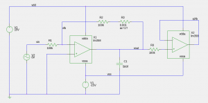
The above example shows an AC analysis test-bench GSCHEM. In this example the loop is broken by R3 whose value at dc is 1mO and is changed to 1TO for ac analysis. Doing this enables NGSPICE to converge on a sensible dc operating point for open loop analysis without any imperfections such as input offset forcing the output to one of the supply rails. [read more at http://education.ingenazure.com/]

Oct 13, 2014

Wearable Sensing and Computing

 Wearable Sensing and Computing 
 05.11.2014 - 06.11.2014
 EPFL Lausanne (CH)

COURSE OBJECTIVES
The course main objective is to inform and discuss in great details the latest advancements in low power sensing technology, energy harvesting and their heterogeneous integration for wearable smart system applications. Technological roadmaps of performance and future evolutions will be presented. The low power wireless communications are discussed from the point of view of existing standards and challenges for reducing the energy per communicated bit. Another objective is to detail some key future applications for wearable sensing and computing with main emphasis on: (1) medical Diagnostics, monitoring and prevention and (2) sports, fitness and activity monitoring applications. We analyze the benefits of autonomous smart system technology from many different points of view, including that of the individual, the physician, health care management, and society in general. We provide a rationale on the role of such technology as a component of the care cycle and the changes it can induce by reinforcing preventive strategies.

AGENDA on-line
Day 1 (09:00 – 17:00):

  • Introduction to wearable technology and energy efficient functions for autonomous smart systems
  • Energy efficient computing technologies and their importance for wearable applications:
  • Wearable low power sensor technology trends
  • Wearable low power communications technologies
  • Wearable energy harvesting technology trends

Day 2 (09:00 – 17:00):

  • Heterogeneous integration: solutions, roadmaps and trends for wearables
  • Context-driven embodiments by wearable systems and related applications and services
  • Market Trends for Mobile and Wearable Technology
  • Wearable autonomous smart systems: Applications to Medical Diagnostics, Monitoring and Prevention Paradigms using Feedback Loops
  • Wearable Technology – Sports, Fitness and Activity Monitoring Applications
Course registration on-line

Oct 7, 2014

[mos-ak] 7th International MOS-AK Workshop; December 12, 2014 at Berkeley

 7th International MOS-AK Workshop
 Berkeley Friday, Dec. 12, 2014 
 Announcement and Call for Papers 
 
 Together with the MOS-AK Workshop Scientific Program Coordinators Larry Nagel and Andrei Vladimirescu as well as Extended MOS-AK TPC Committee, we have pleasure to invite to the 7th consecutive International MOS-AK Workshop which will be held at Berkeley, California, USA, in the IEDM Conference and CMC Meeting timeframe. The event is organized with aims to strengthen a network and discussion forum among experts in the field, enhance open platform for information exchange related to compact/Spice modeling and Verilog-A standardization, bring people in the compact modeling field together, as well as obtain feedback from technology developers, circuit designers, and CAD/EDA tool vendors. 

Venue:
Room 540 in Cory Hall
EECS Department
University of California, Berkeley

Important Dates:
Call for Papers - September 2014
2nd Announcement - October 2014
Final Workshop Program - November. 2014
MOS-AK Workshop - Friday, Dec. 12, 2014
08:30 - 09:00 - On-site Registration 
09:00 - 11:00 - Morning MOS-AK Session
11:00 - 12:00 - CM Standardization Panel
12:00 - 13:00 - Lunch
13:00 - 16:00 - Afternoon MOS-AK Session 

Topics to be covered include the following:
  • Advances in semiconductor technologies and processing
  • Compact Modeling (CM) of the electron devices
  • Verilog-A language for CM standardization
  • New CM techniques and extraction software
  • Open Source TCAD/EDA modeling and simulation
  • CM of passive, active, sensors and actuators
  • Emerging Devices, CMOS and SOI-based memory cells
  • Microwave, RF device modeling, high voltage device modeling
  • Nanoscale CMOS devices and circuits
  • Technology R&D, DFY, DFT and IC Designs
  • Foundry/Fabless Interface Strategies
Abstract Submission:
Authors should submit an abstract using on-line MOS-AK submission form (any related inquiries can be sent to abstracts@mos-ak.org)
http://www.mos-ak.org/berkeley_2014/abstracts.php

On-line free workshop registration:
http://www.mos-ak.org/berkeley_2014/registration.php

Postworkshop publications:
Selected best MOS-AK technical presentation will be recommended for further publication in a special issue of the International Journal of High Speed Electronics and Systems

Extended MOS-AK/GSA Committee

WG06102014

--
You received this message because you are subscribed to the Google Groups "mos-ak" group.
To unsubscribe from this group and stop receiving emails from it, send an email to mos-ak+unsubscribe@googlegroups.com.
To post to this group, send email to mos-ak@googlegroups.com.
Visit this group at http://groups.google.com/group/mos-ak.
For more options, visit https://groups.google.com/d/optout.

Sep 11, 2014

Open Ph D scholarship on semiconductor device modeling

We offer one scholarship for a Ph D student position in the Department of Electronic Engineering in theUniversitat Rovira i Virgili (URV), in TarragonaSpain.

The duration of the grant will be for three years. The monthly salary will be about 1000 Euro/month. The position will start in January 2014.
The candidate should have a Bachelor and Master degree in Electrical Engineering, Electronic Engineering, Telecommunication Engineering or Physics. A good background in Semiconductor Physics, Semiconductor Devices, or Integrated Circuit Design will be highly appreciated.

The work to be done by the candidate will be focused on the development of new techniques of characterization and modeling of novel advanced semiconductor devices, in particular  III-V devices. It will be related to European and national projects in which the hosting group 
(the so-called NEPHOS group) participates. One recent European Union project coordinated by our NEPHOS group is COMON (COmpact MOdelling Network)

The NEPHOS group at URV is one of the most powerful teams in Europe in the area of compact modeling of semiconductor devices.

Required documents for applicants 

Applicants are required to send to the address specified below the following documents (in English or Spanish):
1) a full Curriculum Vitae (as complete as possible) with passport number
2) Copy of their diploma
3) copy of their passport
4) Academic certificate including their marks (it is important that the number of hours or credits of each subject appears) for the subjects studied when pursuing Bachelor Degree and Master degree. It is also very important that the document specifies what is the minimum mark for passing a given subject and what is the maximum mark that can be awarded.
Candidates are requested to send their documents by e-mail to:
Prof. Benjamin IñiguezDepartment of Electronic, Electrical and Automatic Control Engineering
Universitat Rovira i Virgili (URV)
Avinguda Països Catalans, 26
43007 
Tarragona (Spain)Email: benjamin.iniguez@gmail.comTel: +34977558521 Fax:+34977559610

Deadline:  September 18 2014
You can contact Prof. Benjamin Iñiguez (Benjamin.Iniguez@gmail.com) for more information
Tarragona is a medium city (100000 inhabitants) with a Mediterranean climate and many recreation opportunities (nice beaches, theme parks, nature preserves, mountain hiking, touristic resorts and facilities). It is located 100 km Southwest of Barcelona, and it is very well connected by train, bus, highways and even low cost flights from its own airport. Additional information about the University and the department can be found at:www.urv.cat and etse.urv.es

Aug 14, 2014

[mos-ak] [Final Program] 12th MOS-AK Workshop at the ESSDERC/ESSCIRC Conference in Venice

 Autumn MOS-AK Workshop in Venice 
 
 Together with the MOS-AK Workshop Scientific Program Coordinators Larry Nagel and Andrei Vladimirescu as well as Extended MOS-AK TPC Committee, we have pleasure to invite to the 12th consecutive MOS-AK at the ESSDERC/ESSCIRC Conference. 

Venue:
Palazzo del Casinò
Lungomare Marconi, 30
30126 Venice Lido, Italy

MOS-AK Workshop Online Registration 
MOS-AK Workshop Program

08:30-08:50 On-site Registration
08:30-08:50 Morning Session: Open Source CAD/EDA Tools
Is It Time To Rethink the SPICE Input "Language"?
Larry Nagel
Omega Enterprises Consulting (USA)
Parallel Circuit Simulation: How Good Can It Get?
Andrei Vladimirescu
ISEP (FR); UCB (USA)
CUSPICE: The revolutionary NGSPICE on CUDA Platforms
Francesco Lannutti
Sapienza University of Rome (I)
10:30-11:00 Coffee break
Circuit Simulation Update: GPU Progress; Electrothermal Cosimulation
Rick Poore
Keysight Technologies (USA)
QUCS Roadmap
Mike Brinson
QUCS Development (EU)
12:30-13:30 Lunch
13:30-16:30 Afternoon MOS-AK Session: Device Level SPICE/Verilog-A Modeling
Total Virtual Fabrication of Advanced CMOS Devices and Processing
W. Clark, M. Hargrove, G. Schropfer, D. Fried 
Coventor (F)
Performance Comparison of Hall Effect Sensors Obtained by Regular Bulk or SOI CMOS Technology
Maria-Alexandra Paun
University of Cambridge, (UK)
RF Characterization and Modeling of Nanoscale MOSFET from Weak to Strong Inversion
Maria-Anna Chalkiadaki and Christian Enz
EPFL STI IMT ICLAB (CH)
THz Compact Modeling 
Michael Shur
Rensselaer Polytechnic Institute, NY, (USA)
Compact Modeling of Junctionless Cylindrical Nanowires
Benjamin Iniguez
URV, (SP)
Comparative Analysis of SOI/SOS MOSFET SPICE Models with Account for Radiation Effects
Konstantin Petrosyants(1), Igor Kharitonov (1), Lev Sambursky (1,2)
(1) MIEM HSE (RU), (2) IPPM RAS (RU)
16:30 End of the MOS-AK Workshop 

Postworkshop publications:
selected best MOS-AK technical presentation will be recommended for further publication in a special issue of the International Journal of High Speed Electronics and Systems 


--
You received this message because you are subscribed to the Google Groups "mos-ak" group.
To unsubscribe from this group and stop receiving emails from it, send an email to mos-ak+unsubscribe@googlegroups.com.
To post to this group, send email to mos-ak@googlegroups.com.
Visit this group at http://groups.google.com/group/mos-ak.
For more options, visit https://groups.google.com/d/optout.

Aug 11, 2014

Dr. Jindal has been nominated for the Delegate-Elect/Director-Elect 2015

Dr. Renuka Jindal is Professor of Electrical and Computer Engineering at the University of Louisiana at Lafayette, LA, USA since 2002. His research and teaching interests lie in the theory and practice of random processes applicable to a wide variety of phenomena in electronic and photonic devices and circuits, lightwave and wireless communications systems and biological organs. Dr. Jindal was elected Fellow of IEEE in 1991 for his seminal work reducing MOSFET noise by almost an order of magnitude for analog and RF applications. He is also a recipient of the IEEE 3rd Millennium medal. For last four decades of his dual career in industry and academia, Dr. Jindal rose through the ranks as Editor, Editor-in-Chief, VP of Publications, and as EDS President in 2010- 2011. As President he formulated the vision and mission of EDS enhancing member benefits launching a plethora of initiatives reversing the decline in EDS membership. A partial list of his accomplishments is given below:


As Senior-Past President of EDS Dr. Jindal is still very much engaged with IEEE. Recently, Dr. Jindal has been nominated by IEEE Division I to run for the Delegate-Elect/Director-Elect 2015 position in the upcoming IEEE elections. The electorate consists of members of three societies i.e. Electron Devices (ED), Solid-State Circuits (SSC) and Circuits and Systems (CAS). The slate consists of three candidates one from each of these societies. 

On his behalf, I suggest to contact your colleagues in IEEE regions 1-10 for his support since IEEE ballots will be out by August 15.

Jul 30, 2014

Semiconductor Devices Characterization Seminar

Technical Seminars addressing the challenges of CMOS, Power and RF
semiconductor device measurement and modeling 
Agilent and it´s 25 collaborative partners invite you to attend this complimentary technical seminar on characterization and modeling of semiconductor devices. Two tracks in parallel will address the needs for:
  • Small scale silicon industry
  • Power silicon industry and RF Power
Common topics to both Tracks:
  • Live demonstration of GaN device characterization flow: DC I-V characteristic extraction, RF Power measurement, Spice models creation for further usage in design stage.
CMOS Track:
  • Accurate and repeatable on-the-wafer device extraction – Cascade Microtech
  • DC characterization for emerging nano-technologies
  • Flicker Noise and Random Telegraph Noise
  • Spice model libraries optimization for dedicated application
Power & RF Power Track:
  • High Power Devices measurement
  • III-V devices spice model (DynaFET)
  • Nonlinear Component characterization
  • Non-50ohm Load Pull solution – Maury
Where/when:
To obtain the detail agenda of the nearest session, please select one of the locations below.
CountryCityDateMore Information
FRGrenoble18 September 2014Register here
FIHelsinki23 September 2014Register here
DEMunich30 September 2014Register here
DEDresden2 October 2014Register here
CHLausanne14 October 2014Register here
BELeuven16 October 2014Register here
NLEindhoven17 October 2014Register here
SWGoteborg28 October 2014Register here
UKCambridge30 October 2014Register here
FRLes Ulis6 November 2014Register here


Jul 28, 2014

i-MOS version 201407 release

 The i-MOS team has announced new release of the interactive Modeling and On-line Simulation Platform (i-MOS), version 201407. Through the Developer module launched in April, the UMEM model for organic thin film transistors has been integrated with i-MOS for users' evaluations and applications. Another model implemented is the BSIM4 (version 4.0.0), together with model collections from the Predictive Technology Models.  

Any comments and other equerries can be addressed to
Lining Zhang,
PhD i-MOS Project Manager
The Hong Kong University of Science & Technology

Jul 16, 2014

[SISPAD] Compact Modeling Worksops - Enabling Better Insight of Device Features - Monday, September 8, 2014


 SISPAD Compact Modeling Workshop
 Enabling Better Insight of Device Features 
 Monday, September 8, 2014

 Workshop Program

09:15 - 09:20: Opening 

09:20 - 10:00: J. Takeya (University of Tokyo, Japan): invited Physics of Charge Transport in Organic Field-Effect Transistors
10:00 - 10:40: C. Jungemann (RWTH Aachen University, Germany): invited Validity of Macroscopic Noise Models in the Case of High-Frequency Bipolar Transistors
10:40 - 11:00: break
11:00 - 11:40: N. Goldsman (University of Maryland, USA): invited Key Issues in the Modeling of SiC Electronic Devices
11:40 - 12:10: C. Ma (Hiroshima University, Japan): invited Universal Model of the Negative Bias Temperature Instability (NBTI) Effect for Circuit Aging Simulation

12:10 - 12:30: poster presentations
  • P. X. Tran (International University, Vietnam) A Comprehensive Model for the Changing I-V Characteristics of raphene Transistors 
  • M. Ghittorelli, F. Torricelli, Z. M. Kovacs-Vajna, and L. Calalongo (University of Brescia, Italy) Accurate Modeling of Amorphous Indium-Gallium-Zinc-Oxide TFTs Deposited on Plastic Foil 
  • S. Sato, Y. Omura, and A. Mallik (Kansai University, Japan) Proposal of Simple Channel-Length-Dependent Current Model for Subthreshold Region of Nano-Wire Tunnel FET 
  • H. Miyamoto, H. Zenitani, H. Kikuchihara, H. J. Mattausch, M. Miura-Mattausch, and T. Nakagawa (HU & AIST, Japan) Consistent Compact Modeling of MOSFETs from Bulk to Double-Gate Structures
12:30 - 13:50: lunch

13:50 - 14:30: D. Warning (Creative Chips GmbH, Germany): invited NGSPICE – an Open Platform for Modeling and Simulation
14:30 - 15:00: A. Schaldenbrand (Cadence Design Systems, Japan): invited Benefits of Verilog-A for Behavioral Modeling and Compact Modeling
15:00 - 15:30: P. Lee (Micron Memory Japan, Inc.): invited Compact Model Coalition: World-Wide Model Standardization for an Expanding Industry

15:30 - 15:40: break

15:40 - 16:00: F. Torricelli, M. Ghittorelli, M. Rapisarda, L. Mariucci, S. Jacob, R. Coppard, E. Cantatore, Z. M. Kovacs-Vajna, and L. Colalongo (Unviersity of Brescia, Italy) Analytical Drain Current Model of Both p- and n-Channel OTFTs for Circuit Simulation
16:00 - 16:20: T. Nakagawa, T. Sekigawa, M. Hioki, Y. Ogasahara, H. Koike, H. Zenitani, H. Miyamoto, H. Kikuchihara, H. J. Mattausch, M. Miura-Mattausch, H. Oda, and N. Sugii (AIST, HU, LEAP, Japan) Parameter-Extraction Strategy of Ultra-Thin Silicon and BOX Layer MOSFETs for Low Voltage Applications
16:20 - 16:40: T. Mizoguchi, T. Naito, Y. Kawaguchi, and W. Hatano (Toshiba, Japan) Compact Modeling of GaN-MISFET for Power Applications
16:40 - 17:00: T. Yamamoto and H. Kato (Denso, Japan) Analysis and Modeling of Injection Enhanced Insulated Gate Bipolar Transistor

17:00: Closing

Jun 11, 2014

ESSDERC/ESSCIRC 2014 - Full conference program is now available

The technical programtutorial program, and workshop program of ESSDERC/ESSCIRC 2014
are now available at  ESSDERC/ESSCIRC 2014  website: http://www.esscirc-essderc2014.org 

Please remember to register to the conference and book a hotel room at before June 20, after 
which we cannot guarantee that you will find a hotel room at our rebated prices.
The event is technically co-sponsored by the
    IEEE Electron Device Society,
    IEEE Solid-State Circuit Society
    IEEE Circuits and Systems Society


We hope to see you in Venice

Best Regards
  Gaudenzio Meneghesso
ESSDERC/ESSCIRC 2014  General Chair

Roberto Bez and Paolo Pavan
ESSDERC 2014 TPC Chairs

Pietro Andreani and Andrea Bevilacqua 
ESSCIRC
 
2014 TPC Chairs


JOINT PLENARY TALKS 
Scott DeBoer
, Micron, ID, USA, A Semiconductor Memory Manufacturing and Development Perspective
Thomas H. Lee
, Stanford University, CA, USA Terahertz Electronics: The Last Frontier 
Fabio Marchiò
, STMicroelectronics, Italy, Automotive Electronics: Application & Technology Megatrends
Walter Snoeys
, CERN, Switzerland, How Chips Helped Discover the Higgs Boson at CERN
An Steegen
, IMEC, Belgium, Logic Scaling Beyond 10nm, a Power-Performance-Area-Cost Trade-off 
Sehat Sutardja
, Marvell Semiconductor, CA, USA Tremendous Benefits of Moore’s Law Have Yet to Come
ESSCIRC PLENARY TALKS
Hooman Darabi
, Broadcom Corporation, CA, USA Blocker Tolerant Software Defined Receivers
Un-Ku Moon, Oregon State University, OR, USA Emerging ADCs
Kathleen Philips
, IMEC-Holst Centre, The Netherlands Ultra-Low Power Short Range Radios
ESSDERC PLENARY TALKS
Umesh Mishra
, UCSB and TRanphorm, CA, USA,  GaN-based solutions from KHz to THz 
Eric Pop, Stanford University, CA, USA, Energy Efficiency and Conversion in 1D and 2D Electronics
Takao Someya
, University of Tokyo, Japan Bionic Skins Using Flexible Organic Devices

ESSCIRC TUTORIALS
Power Management for SoCs (Full Day), Organizer: Christoph Sandner, Infineon, Austria
High Performance Amplifiers 
(Half Day), Organizer: Angelo Nagari, STMicroelectronics, France
Phase Noise: from Fundamentals to Circuit Aspects (Half Day) Organizer: Christian Enz, EPFL, Switzerland
ESSDERC TUTORIALS
CMOS Technology at the nm Scale Era 
(Full Day) Organizer: Maud Vinet, CEA LETI, France
RRAM: from Technology to Applications (Half Day) Organizer: Bogdan Govoreanu, IMEC, Belgium 
3D: from Technology to Applications 
(Half Day) Organizer: Pascal Vivet, CEA LETI, France

ESSDERC/ESSCIRC Workshops
Beyond-CMOS for advanced More Moore and More than Moore applications
 
Organizers: Francis Balestra and Enrico Sangiorgi, Sinano Institute - Grenoble INP/CNRS, France
MOS-AK: Over Two Decades of Enabling Compact Modeling R&D Exchange   
Organizer: Wladek Grabinski, MOS-AK Group (EU),
Status of the GaN and SiC based device development
   
Organizer: Enrico Zanoni, University of Padova, DEI, Italy
THz-Workshop: Millimeter- and Sub-Millimeter-Wave circuit design and characterization
   
Organizer: Thomas Zimmer, University Bordeaux, France
Marie Curie ATWC
   
Organizer: Rinaldo Castello, University of Pavia and Marvell, Italy

May 18, 2014

[mos-ak] 12th MOS-AK Workshop at the ESSDERC/ESSCIRC Conference in Venice

 Autumn MOS-AK Workshop in Venice 
 
Together with the MOS-AK Workshop Scientific Program Coordinators Larry Nagel and Andrei Vladimirescu as well as Extended MOS-AK TPC Committee, we have pleasure to invite to the 12th consecutive MOS-AK at the ESSDERC/ESSCIRC Conference.

Venue:
Palazzo del Casinò
Lungomare Marconi, 30
30126 Venice Lido, Italy

Important Dates:
Call for Papers - May 2013
2nd Announcement - June 2014
Final Workshop Program - Aug. 2014
MOS-AK Workshop - Friday, Sept. 26, 2014
 8:30 -  9:00 - On Site Registration
 9:00 - 12:00 - Morning MOS-AK Session
12:00 - 13:00 - Buffet Lunch  
13:00 - 16:00 - Afternoon MOS-AK Session

Topics to be covered include the following:
Advances in semiconductor technologies and processing
Compact Modeling (CM) of the electron devices
Verilog-A language for CM standardization
New CM techniques and extraction software
Open Source TCAD/EDA modeling and simulation
CM of passive, active, sensors and actuators
Emerging Devices, CMOS and SOI-based memory cells
Microwave, RF device modeling, high voltage device modeling
Nanoscale CMOS devices and circuits
Technology R&D, DFY, DFT and IC Designs
Foundry/Fabless Interface Strategies

Abstract Submission:
Authors should submit an abstract using on-line MOS-AK submission form (any related enquiries can be sent to abstracts@mos-ak.org)

Postworkshop publications:
selected best MOS-AK technical presentation will be recommended for further publication in a special issue of the International Journal of High Speed Electronics and Systems


[WG 052014]

--
You received this message because you are subscribed to the Google Groups "mos-ak" group.
To unsubscribe from this group and stop receiving emails from it, send an email to mos-ak+unsubscribe@googlegroups.com.
To post to this group, send email to mos-ak@googlegroups.com.
Visit this group at http://groups.google.com/group/mos-ak.
For more options, visit https://groups.google.com/d/optout.

May 5, 2014

IJNM Call for Papers

Advances in simulation-driven modeling and optimization of microwave/RF circuits
IJNM Call for Papers

Computer-aided modeling and design of microwave/radio frequency (RF) devices and circuits have undergone tremendous developments in the past decade. The complexity of today's devices and circuits renders electromagnetic (EM) simulation a sine qua non in the microwave design process. That said, EM-driven design poses significant challenges, mostly due to the high computational cost of accurate, high-fidelity simulation. The availability of massive computational resources does not always translate into design speedup because of the need to account for interactions between devices and their surroundings as well as multi-physics (e.g., EM-thermal) effects. Not surprisingly, traditional design optimization procedures that directly utilize EM-simulated responses typically fail or are impractical. As a consequence, there is growing interest in alternative optimization and modeling methodologies, especially ones that exploit computationally cheap surrogate models.
This Special Issue focuses on the current state of the art and future directions in microwave and RF design. Papers on software engineering and practical applications aspects are also encouraged. Suitable topics for this Special Issue therefore include but are not limited to
  • surrogate-based modeling and optimization methods including space mapping;
  • knowledge-based and tuning methodologies;
  • global optimization, evolutionary algorithms, particle swarm optimization, and so on;
  • multi-objective optimization;
  • adjoint-sensitivities for efficient gradient-based optimizers;
  • optimization techniques for nonlinear circuits;
  • software architectures for optimization-oriented design;
  • automated design optimization using EM simulators;
  • optimization for inverse EM problems;
  • neural network approaches; and
  • optimization for discrete problems.
Manuscripts for this Special Issue should adhere to the requirements for regular papers of the IJNM as specified in the Author Guidelines at http://onlinelibrary.wiley.com/journal/10.1002/(ISSN)1099-1204/homepage/ForAuthors.html
Potential contributors may contact the guest editor to determine the suitability of their contribution to the Special Issue. All manuscripts should be submitted via the IJNM's manuscript website http://mc.manuscriptcentral.com/ijnm, with a statement that they are intended for this Special Issue.

Manuscript submission deadline: January 31, 2015

Prof. Slawomir Koziel
Engineering Optimization and Modeling Center, 
School of Science and Engineering, 
Reykjavik University, Reykjavik, Iceland

May 4, 2014

[mos-ak] [Summary] Spring MOS-AK Workshop in London

 MOS-AK Compact Modeling Workshop
 London Metropolitan University
 March 28-29, 2014 London
 
The MOS-AK/GSA Modeling Working Group, a global compact modeling standardization forum, delivered its annual spring compact modeling workshop on March 28-29, 2014 at London Metropolitan University. The event received full sponsorship from leading industrial partners including Agilent Technologies, MOSIS Services and Tanner EDA. The technical MOS-AK program promoters included Eurotraining, IET, IEEE UKRI Section as well as EDA Solutions. More than 40 registered academic researchers and modeling engineers attended two sessions to hear 9 technical compact modeling presentations including the QUCS Tutorial by Prof. Mike Brinson.
 
The workshop summary has been posted thru the semiwiki.com blog and all the MOS-AK presentations are available for downloads here.
 
The MOS-AK/GSA Modeling Working Group is coordinating several upcoming modeling events to focus on the Verilog-A compact model standardization as well as open source circuit simulation tool developments: 
In the meantime, please also visit www.mos-ak.org where we will continue the discussions of all compact/SPICE modeling topics and its Verilog-A standardization.

--WG--V2014

--
You received this message because you are subscribed to the Google Groups "mos-ak" group.
To unsubscribe from this group and stop receiving emails from it, send an email to mos-ak+unsubscribe@googlegroups.com.
To post to this group, send email to mos-ak@googlegroups.com.
Visit this group at http://groups.google.com/group/mos-ak.
For more options, visit https://groups.google.com/d/optout.

Apr 27, 2014

[mos-ak] CUSPICE: CUDA-accelerated NGSPICE release available immediately

 Recently, Francesco Lannutti, NGSPICE lead developer, has announced the CUSPICE: CUDA-accelerated NGSPICE release. The NVIDIA has recognised importance of the open source CAD/EDA tools and gave the permission to release CUSPICE as an integral part of the NGSPICE simulation platform. New NGSPICE extension is available immediately on the NGSPICE repository, in the branch named 'CUSPICE'. 

 At the moment only BSIM4v7, CAP, IND, ISRC, RES and VSRC device models are supported by the CUSPICE simulator. With broad acceptance of the NGSPICE simulation platform, we can expect other standard models and new extensions developed, soon. 

--
You received this message because you are subscribed to the Google Groups "mos-ak" group.
To unsubscribe from this group and stop receiving emails from it, send an email to mos-ak+unsubscribe@googlegroups.com.
To post to this group, send email to mos-ak@googlegroups.com.
Visit this group at http://groups.google.com/group/mos-ak.
For more options, visit https://groups.google.com/d/optout.

Apr 21, 2014

[Abstracts Due Extended] 2014 NanoTech Workshop on Compact Modeling


 NanoTech Workshop on Compact Modeling Important Dates:
  • Late Poster Abstracts Due: Rolling Submissions - May 15
  • Notification: Rolling Notification Date
Authors of research submissions, upon acceptance, must register for the conference. [read more...]

Apr 17, 2014

Devices That You Definitely Will (and Just Might) Use: Emerging Transistor Technologies for the Near-and Long-Term

 WEDNESDAY June 04, 4:00pm - 6:00pm | Room 302 
 TRACK: EDA
 TOPIC AREA: EMERGING TECHNOLOGIES

 SPECIAL DAC SESSION 63: Devices That You Definitely Will (and Just Might) Use: Emerging Transistor Technologies for the Near-and Long-Term

Chair:  Michael Niemier; Univ. of Notre Dame, IN
Organizers:  Michael Niemier; Univ. of Notre Dame, IN
Xiaobo Sharon Hu; Univ. of Notre Dame, IN

Want to learn about the latest developments in FinFET-based processor design? What other transistor technologies might follow FinFETs and would they bring new design and modeling challenges? Come to this session to hear about both near- and long-term transistor technologies and their prospects for continuing Moore’s Law-based performance scaling trends. The session will begin with a discussion of FinFET technology; subsequent presentations will discuss tunnel transistors (TFETs) as well as other emerging FET technologies that could reenable voltage scaling. The session will conclude with a discussion of modeling efforts that consider the impact of new device technologies on von Neumann architectures as well as hybrid analog/digital circuits and architectures.

63.1 FinFET's and Their Implications for Design Now and in the Future

  • Speaker: Rob Aitken; ARM Ltd., San Jose, CA
    Greg Yeric; ARM Ltd., Austin, TX
    Brian Cline; ARM Ltd., Austin, TX
    Lucian Shifren; ARM Ltd., San Jose, CA

63.2 Emerging Devices for Logic: Can a Low-Power Switch Be Fast?

  • Speaker: Thomas Theis; IBM T.J. Watson Research Center, Yorktown Heights, NY

63.3 Energy Efficient Tunnel-FET Transistors for Beyond CMOS Logic

  • Speaker: Uygar Avci; Intel Corp., Portland, OR
    Daniel Morris; Intel Corp., Portland, OR
    Ian Young; Intel Corp., Hillsboro, OR

63.4 Steep Slope Devices: Enabling New Architectural Paradigms

  • Speaker: Vijaykrishnan Narayanan; Pennsylvania State Univ., State College, PA
    Karthik Swaminathan; Pennsylvania State Univ., State College, PA
    Huichu Liu; Pennsylvania State Univ., State College, PA
    Moon Seok Kim; Pennsylvania State Univ., State College, PA
    Xueqing Li; Pennsylvania State Univ., State College, PA
    Jack Sampson; Pennsylvania State Univ., University Park, PA