Dec 24, 2020

[paper] IGBT Compact Modeling

Compact Modeling of IGBT Charging/Discharging for Accurate Switching Prediction
Y. Miyaoku1, A. Tone1, K. Matsuura1, M. Miura-Mattausch1 (Fellow, IEEE),
H. J. Mattausch1 (Senior Member, IEEE), and D. Ikoma2
IEEE J-EDS, vol. 8, pp. 1373-1380, 2020
doi: 10.1109/JEDS.2020.3008919
1 Graduate School of Advanced Sciences of Matter, Hiroshima University, Higashi-Hiroshima 739-8527, Japan
2 Sensor and Semiconductor Development, Denso Corporation, Aichi 448-8661, Japan


ABSTRACT The trench-type IGBT is one of the major devices developed for very high-voltage applications, and has been widely used for the motor control of EVs as well as for power-supply systems. In the reported investigation, the accurate prediction of the power dissipation of IGBT circuits has been analyzed. The main focus is given on the carrier dynamics within the IGBTs during the switching-off phase. It is demonstrated that discharging and charging at the IGBT’s gate-bottom-overlap region, where electron discharging is followed by hole charging, has an important influence on the switching performance. In particular, the comparison of long-base and short-base IGBTs reveals, that a quicker formation of the neutral region within the resistive base region, as occurring in the long-base IGBT, leads to lower gatebottom-overlap capacitance, thus realizing faster electron discharging and hole charging of this overlap region.
FIG: IGBT structures with nMOSFET + pnp BJT part (a. and b.) and nMOSFET-only structure (c.). The X–Y line is through the middle of the bottom-gate oxide and the A–B line is directly underneath the bottom-gate oxide.

Received 14 May 2020; revised 2 July 2020; accepted 8 July 2020. Date of publication 13 July 2020; date of current version 8 December 2020. The review of this article was arranged by Editor M. Mierzwinski. Digital Object Identifier 10.1109/JEDS.2020.3008919


Dec 23, 2020

[paper] Coplanar OTFT

Blurred Electrode for Low Contact Resistance in Coplanar Organic Transistors
Xiaolin Ye, Xiaoli Zhao, Shuya Wang, Zhan Wei, Guangshuang Lv, Yahan Yang, Yanhong Tong, Qingxin Tang, and Yichun Liu
American Chemical Society; Nano; Dec.18, 2020
DOI: 10.1021/acsnano.0c08122

*Center for Advanced Optoelectronic Functional Materials Research, and Key Lab of UV-Emitting Materials and Technology of Ministry of Education, Northeast Normal University, 5268 Renmin Street, Changchun 130024, China

Abstract: Inefficient charge injection and transport across the electrode/semiconductor contact edge severely limits the device performance of coplanar organic thin-film transistors (OTFTs). To date, various approaches have been implemented to address the adverse contact problems of coplanar OTFTs. However, these approaches mainly focused on reducing the injection resistance and failed to effectively lower the access resistance. Here, we demonstrate a facile strategy by utilizing the blurring effect during the deposition of metal electrodes, to significantly reduce the access resistance. We find that the transition region formed by the blurring behavior can continuously tune the molecular packing and thin-film growth of organic semiconductors across the contact edge, as well as provide continuously distributed gap states for carrier tunnelling. Based on this versatile strategy, the fabricated dinaphtho[2,3-b:2′,3′-f]thieno[3,2-b]thiophene (DNTT) coplanar OTFT shows a high field-effect mobility of 6.08 cm2 V–1 s–1 and a low contact resistance of 2.32 kΩ cm, comparable to the staggered OTFTs fabricated simultaneously. Our work addresses the crucial impediments for further reducing the contact resistance in coplanar OTFTs, which represents a significant step of contact injection engineering in organic devices.

Fig: Coplanar Organic Transistors (oTFTs)


Dec 22, 2020

[Highlights] 2020 IEEE IEDM


The IEEE International Electron Devices Meeting (IEDM), which this year was organized online (December 12-18, 2020), is a key forum for reporting developments in semiconductor and electronic device technology. 
Nature Electronics Research Highlights
 
Gate-all-around transistors stack up
by Stuart Thomas; Nature Electronics 

Gallium nitride gets wrapped up
by Stuart Thomas; Nature Electronics 

Vacuum transistors with high-power operation
Matthew Parker; Nature Electronics 

Beam scanning on a single chip
Matthew Parker; Nature Electronics 

FinFETs for cryptography
Christiana Varnava; Nature Electronics 

Electronics in an organic package
Christiana Varnava; Nature Electronics 

[mos-ak] [online publications] Virtual International MOS-AK Workshop, Silicon Valley, Dec. 10-11, 2020


Local organization THM Team together with the International MOS-AK Board of R&D Advisers as well as all the Extended MOS-AK TPC Committee have organized two days virtual/online event:
  • 13th International MOS-AK Workshop,  Silicon Valley, Dec. 10-11, 2020
    • virtual session 11:00 - 14:00 (PST) on Dec.10, 2020
    • virtual session 11:00 - 14:00 (PST) on Dec.11, 2020
Online Publications:
There are MOS-AK technical presentations covering selected aspects of the compact/SPICE modeling and its Verilog-A standardization (see all the slide presentations online at corresponding link).

Postworkshop Publications:
Selected, best MOS-AK technical presentation will be recommended for further publication in a special Solid State Electronics issue on compact modeling planned for the next 2021 year.

The MOS-AK Association plans to continue its standardization efforts by organizing future compact modeling meetings, workshops and courses around the globe thru the next 2021 year, including:
  • 1st MOS-AK Asia/South Pacific, (online) end Feb.2021
  • 3rd MOS-AK/India Conference, Hyderabad (IN) Rescheduled 2021
  • MOS-AK at LAEDC (MX), April 18-20 2021
  • FOSS TCAD/EDA at 5NANO2021, Kottayam (IN) April, 2021
  • 5th Sino MOS-AK Xi'an (CN),  Rescheduled 2021
  • WCM at the Nanotech, Washington DC (US), Rescheduled 2021
  • IRPhE, mmW and THz Conf. Aghveran (AM) Rescheduled 2021
  • 19th MOS-AK at ESSDERC/ESSCIRC, Grenoble (F) Sept. 2021
  • 14th US MOS-AK Workshop, Silicon Valley (US) Dec. 2021
    in timeframe of IEDM and Q4 CMC Meetings
W.Grabinski on the behalf of International MOS-AK Committee 
WG221220

[paper] Radiation testing of a 6-axis MEMS inertial navigation unit

Radiation testing of a commercial 6-axis MEMS inertial navigation unit at ENEA Frascati proton linear accelerator
G. Bazzanoa,b, A. Ampollinia, F. Cardellia, F. Fortinia, P. Nenzia, G.B. Palmerinib, L. Picardia
L. Piersantia, C. Ronsivallea, V. Surrentia, E. Trincaa, M. Vadruccia, M. Sabatinic
Advances in Space Research (2020)
DOI: 10.1016/j.asr.2020.11.031
aENEA, Via Enrico Fermi 45, Frascati, Italy
bScuola di Ingegneria Aerospaziale, La Sapienza Università di Roma, Italy
cDipartimento di Ingegneria Astronautica, Elettrica ed Energetica, La Sapienza Università di Roma, Italy 

Abstract: We present the first results of a novel collaboration activity between ENEA Frascati Particle Accelerator Laboratory and University La Sapienza Guidance and Navigation Laboratory in the field of Radiation Hardness Assurance (RHA) for space applications. The aim of this research is twofold: (a) demonstrating the possibility to use the TOP-IMPLART proton accelerator for radiation hardness assurance testing, developing ad hoc dosimetric and operational procedures for RHA irradiations; (b) investigating system level radiation testing strategies for Commercial Off The Shelf (COTS) components of interest for SmallSats space missions, with focus on devices and sensors of interest for guidance, navigation and control, through simultaneous exploration of Total Ionizing Dose (TID), Displacement Damage (DD) dose and Single-Event Effects (SEE) with proton beams. A commercial 6-axis integrated Micro Electro-Mechanical Systems (MEMS) inertial navigation system (accelerometer, gyroscope) was selected as first Device Under Test (DUT). The results of experimental tests aimed to define an operational procedure and the characterization of radiation effects on the component are reported, highlighting the consequence of the device performance degradation in terms of the overall navigation system accuracy. Doses up to 50 krad(Si) were probed and cross sections for Single-Event Functional Interrupt (SEFI) evaluated at a proton energy of 30 MeV. 
Fig: Polyedric support for MEMS accelerometer characterization


Dec 21, 2020

[paper] Cross Domain Modeling of a Meander Beam MEMS Accelerometer

Mahdieh Shojaei Baghini*

*Department of Mechanical, Maritime and Materials Engineering, Delft University of Technology, Delft, Netherlands

Abstract: This paper presents the design of a bulk Silicon MEMS single-axis 8-beam accelerometer utilizing meander beams in the Structural Mechanics and MEMS Module of COMSOL Multiphysics®. To obtain further insights into the design of the accelerometer, an electrical lumped element model of the structure is derived and represented in SPICE. Quantities such as eigenfrequencies and proofmass displacement have been extracted from COMSOL Multiphysics® as well as analytical studies. The effects of parasitic frequencies in the structure are observed by automatic tilting of the accelerometer at higher order eigenfrequencies due to finite off-axis stiffness coefficients. In order to mathematically quantify the response of the accelerometer arising due to parasitic frequencies, the transient damping response has been derived in COMSOL Multiphysics® as well as SPICE, and the differences are highlighted. Finally, the eigenfrequencies of the meanderbeam accelerometer have been compared with that of a simple-beam accelerometer and the validity of small deflection theory is tested for the lumped model approach. While the target damping factor of the accelerometer was 0.7, the obtained damping factor increased to 1.1 due to the aforementioned parasitic frequencies and reduction in the resonance frequency of the sensor. This effect was precisely captured during the COMSOL Multiphysics® simulation.
Fig: The designated sensor is damped using plates placed at a distance equal to h0; its a) electrical circuit equivalent of squeeze-film damped accelerometer; b) electrical circuit considering symmetric damping; c) simplified equivalent circuit for gap height derivation.


Dec 15, 2020

[VIRTUAL] EDS MQ on Compact Modeling

VIRTUAL MINI-COLLOQUIUM ON COMPACT MODELING


IEEE EDS Compact Modeling Technical Committee
EDS Spain Chapter
Department of Electronic, Electrical and Automatic Control Engineering, 
University Rovira I Virgili, Tarragona (Spain)

December 17, 2020
EDS MQ Program (times in CET)
10:20-10:30
Benjamin Iñiguez, IEEE EDS MQ Chair
Department of Electronic, Electrical and Automatic Control Engineering, University Rovira I Virgili, Tarragona (Spain)
Opening session
10:30-11:15
Yogesh. S Chauhan
Department of Electrical Engineering,
Indian Institute of Technology Kanpur (India)
BSIM-BULK and BSIM-HV: Industry Standard SPICE Models for Analog, RFand High Voltage Applications
11:15-12:00
Manoj Saxena
Department of Electronics, University of Delhi  (India)
“Modeling and Simulation of Robust Ultrasensitive Tunnel Field Effect Transistor Design for Biosensing Applications”
12·00-12:45
Wladek Grabinski
GMC, Commugny (Switzerland)
FOSS TCAD/EDA Tools for Semiconductor Device Modeling
12:45-13:30
Arokia Nathan
Darwin College, University of Cambridge (UK)
“Physics-Based Parameter Extraction for TFTs”
13:30-15:00 Break
15:00-15:45
Marcelo Pavanello
Department of Electrical Engineering,
Centro Universitario FEI, Sao Bernardo do Campo (Brazil)
"Quantum Effects on the Mobility of SOI Nanowire MOSFETs Induced by the Active Substrate Bias"
15:45-16:30
Michael S. Shur
Department of Electrical, Systems and Computer Engineering,
Rensselaer Polytechnic Institute, Troy NY (USA)
THz Compact SPICE/ADS model
16:30-17:15
Edmundo Gutiérrez
Department of Electronics, INAOE, Puebla (Mexico)
"RF MOSFET degradation modeling up to 67 GHz”
End of EDS MQ

Dec 12, 2020

[2nd Day Photos] 13th International MOS-AK Workshop

13th International MOS-AK Workshop was organized jointly with THM Giessen who has provided ZOOM meeting platform for the online event. 50+ registered participants have attended 2nd day with two further MOS-AK sessions and followed 7 technical talks

MOS-AK session III - 11:00 - 14:00 (PST) on Dec.11, 2020
Chair: Anurag Mangla; Semtech Neuchatel (CH)

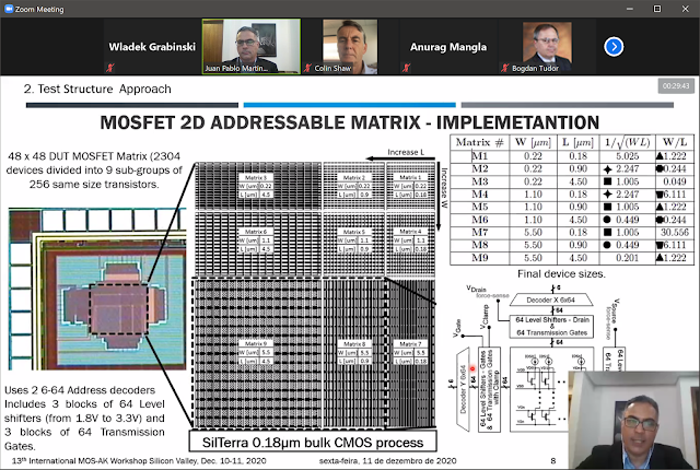
[8] Statistical Analysis of MOSFET extracted parameters for n-MOS mismatch modeling.
Juan Pablo Martinez Brito
CEITEC SA/UFRGS (BR)

[9] Rapid multiscale simulation of nanoscale MOSFETs: Is an interplay between compact models and NEGF possible?
Alexander Kloes
NanoP, THM University of Applied Sciences (D)


[10] The Effect of Non Rectangular MOS Channels in Modelling High Voltage Lateral MOS
Marco Sambi, Lorenzo Labate, Simona Cozzi, Nicola Holzer
STMicroelectronics (I)

MOS-AK session IV
Chair: Daniel Tomaszewski, Lukasiewicz - IMiF, Warsaw (PL)

[11] Nonlinear Embedding Model for the Accelerated Design of PAs with the ASM-HEMT model
Patrick Roblin*, Miles Lindquist*, Nicholas Miller+ and Marek Mierzwinski^
*The Ohio State University, AFRL+, Keysight Corp.^ (USA)

[12] New analytical model for AOSTFTs
Antonio Cerdeira, Yoanlys Hernandez-Barrios, Magali Estrada, Benjamin Iniguez
CINVESTAV (MX) and URV (SP)

[13] Unifying the Modeling of Charge Trapping in RTN, 1/f Noise and BTI
Gilson Wirth
UFRGS (BR)

[14] SPICE Modeling for Display Technologies
Bogdan Tudor
Silvaco (USA)

MOS-AK attendees group photo of 2nd MOS-AK workshop day:

MOS-AK attendees group photo (1)

MOS-AK attendees group photo (2)


Dec 11, 2020

[1st Day Photos] 13th International MOS-AK Workshop


13th International MOS-AK Workshop was organized jointly with THM Giessen who has provided ZOOM meeting platform for the online event. More than 50 registered participants have attended two MOS-AK sessions and followed 7 technical talk during its first day.

MOS-AK session I - 11:00 - 14:00 (PST) on Dec.10, 2020
Chair: Laurie E. Calvet; CNRS-University Paris-Saclay (F)

[1] Material Growth, Characterization of III-V & II-VI Compound Semiconductors and its Use for Various Device Applications
Saxena Praveen Kumar
Tech Next Lab Pvt Ltd (IN)

[2] Contact-controlled transistors: Device characteristics and modelling challenges
Radu Sporea
Uni. Surrey (UK)

[3] Contact-controlled transistors: Specific applications and opportunities
Eva Bestelink
Uni. Surrey (UK)

MOS-AK session II
Chair: Larry Nagel; Omega Enterprises Consulting (USA)

[4] 90 Years of Twoport Matrices and its Impact on Device Measurements and Modeling
Franz Sischka
SisConsult Engineering Office (D)

[5] Some issues on the high-frequency compact modeling of CMOS transistors and related devices
Roberto Murphy
INAOE (MX)

[6] VAMPyRE: Verilog-A Model Pythonic Rule Enforcer
Geoffrey Coram
Analog Devices, Inc. (USA)

[7] Simulate 40X Faster with SmartSpice HPP
Jody Matos
Silvaco (USA)

MOS-AK attendees group photo of 1st MOS-AK workshop day:

MOS-AK attendees group photo (1)

MOS-AK attendees group photo (2)


IEEE Connecting Experts


Dear IEEE Young Professionals,
as part of our IEEE Connecting Experts program, together with IEEE Croatia Section, we are bringing you a panel about design thinking in STEM area and project-based education through interdisciplinary teams, going beyond engineering, to prepare students for the marketplace. The technical talk entitled "Interdisciplinary Project-based Learning" is organized in collaboration with IEEE Croatia Section and is starting tomorrow, December 11 at 15:10 UTC.

MS Teams details
You can join the session here.

About the topic
In this interactive session, the development, design, and implementation of an interdisciplinary project-based learning approach at the WSU will be presented and discussed by the team who designed it and tested its performance. The project called SOAR (STEM-Oriented Alliance for Research) offers a transformative educational experience to students, merging coursework across three different academic disciplines. Science, Technology, Engineering, and Math (STEM) education has been challenged by industries to incorporate business and communication experiences (and vice versa) that prepare students for the workplace. Incorporating interdisciplinary project-based coursework provides experiential learning for students, a skillset that employers indicate as desirable.
The data obtained during the work on the SOAR project suggest that the collaboration in interdisciplinary project-based learning does initially produce disorientation, some trepidation, and confusion. However, ultimately these disorienting dilemmas lead to transformative learning, increased confidence, and cohesion among disciplines. The results of this paper will inform and guide engineering educators in creating interdisciplinary project-based coursework that meets the growing demands of the workplace of today and the future.
To engage in the interactive part of the session, you will need the link: www.pollev.com/jmurray180
All this project, and this Workshop, really is about is how to make students engage their full creativity potentials and make learning more interesting and, ultimately, useful and applicable in the fast-changing economy and society. 

About the speakers
It is our pleasure to host a wonderful team of professors from the Washington State University, Everett:
  • Prof. Lucrezia Cuen Paxson, Clinical Assistant Professor, Edward E. Murrow College of Communication,
  • Dr. Mark Beattie, Associate Vice Chancellor for Academic Affairs and Clinical Assistant Professor in the School of Hospitality Business Management,
  • Dr. Jacob Murray, Clinical Assistant Professor and Program Coordinator for the School of Electrical Engineering and Computer Science,
  • Dr. Soobin Seo, Assistant Professor of hospitality business management at the WSU Everett.

You can check our real-time schedule of talks in the IEEE Connecting Experts Calendar and follow us and our live streams on our Facebook page or YouTube channel.  

Kind regards,
Dubravko Sabolic - IEEE Croatia Section
Vinko Lesic - IEEE Region 8 Young Professionals

Dec 10, 2020

[Foreword] Special Issue on Compact Modeling of Semiconductor Devices

Foreword
Special Issue on Compact Modeling of Semiconductor Devices
DOI: 10.1109/JEDS.2020.3039023

THIS Special Issue is dedicated to recent research in the field of compact modeling of semiconductor devices. This is the first J-EDS Special Issue on compact modeling. In the last years, a number of new semiconductor device structures, for electronic and photonic applications, have been developed. Compact models are needed for the incorporation of these new devices in integrated circuits. Therefore, a Special Issue was needed to present recent compact modeling solutions for semiconductor devices

A total of 8 regular papers and 2 invited papers have been accepted in this Special Issue. All papers, including the invited ones, were subjected to a thorough peer reviewing. A high number of reviewers participated in this process. This has resulted in a Special Issue containing very high-quality papers.  The published papers target compact modeling aspects for a wide number of devices, such as SiGe HBTs, IGBTs, SiC SB diodes, LDMOSFETs, Multi-Gate MOSFETs, RRAMs, TFET SRAMs, and organic TFTs. Open source Verilog-A compil- ing is also targeted by one paper. Different operation regimes and conditions are addressed: charging/discharging, THz, high power, tunneling radiation environments, . . . 

One invited paper, by U. Sharma and S. Mahapatra, addresses the modeling of HCD Kinetics for full VG/VD span under different experimental conditions across architectures and its SPICE implementation The other invited paper, by Fregonese et al., presents a review of THz characterization and modeling of SiGE HBTs.

I [BJ] would like to thank the work done by the rest of the Editors of this Special Issue and also by all the reviewers who participated in this process. And of course, I want to thank all the authors for their interest in submitting papers to this Special Issue. Thanks to authors, reviewers, and editors, this high-quality Special Issue has been possible.

BENJAMIN IÑIGUEZ, Guest Editor-in-Chief
Department of Electronic, Electrical and
Automatic Control Engineering
University Rovira i Virgili
43007 Catalonia, Spain

YOGESH SINGH CHAUHAN, Guest Associate Editor
Department of Electrical Engineering
Indian Institute of Technology Kanpur
Kanpur 208016, India

SLOBODAN MIJALKOVIC, Guest Associate Editor
Simulation Group
EDA Division
Silvaco Europe Ltd.
Cambridgeshire PE27 5JL, U.K.

KEJUN XIA, Guest Associate Editor
Department of Front End Innovation
NXP Semiconductors
Chandler, AZ 85224 USA
JUNG-SUK GOO, Guest Associate Editor
Department of Compact Model Development
GLOBALFOUNDRIES Inc.
Santa Clara, CA 95054 USA

MARCELO PAVANELLO, Guest Associate Editor
Department of Electrical Engineering
Centro Universitario FEI
09850-901 São Bernardo do Campo, Brazil

MAREK MIERZWINSKI, Guest Associate Editor
Department of PathWave Software and Solutions
Keysight Technologies
Santa Rosa, CA 95403 USA
(e-mail: )

WLADEK GRABINSKI, Guest Associate Editor
Department of Research and Development Modelling
GMC Consulting
1291 Commugny, Switzerland

Dec 9, 2020

James D. Meindl, master of integrated circuits, dies at 87

Meindl was a visionary engineer who saw the potential of integrated circuits and was an early proponent of an interdisciplinary approach to engineering research [read more by Andrew Myers]

In 1984, electrical engineering professors James D. Meindl (right) and John Hennessy (center) brainstorm with research engineer John Shott about the MIPS project, which simplified computers with RISC architecture. (Image credit: Chuck Painter / Stanford News Service)

Dec 8, 2020

Solid-State Electronics Editorial Board

Solid-State Electronics Editorial Board
DOI: 10.1016/S0038-1101(20)30401-9


FOUNDING EDITOR
Dr W. Crawford Dunlap

EDITORS
Enrique Calleja
Dept. of Electronic Engineering (ISOM), 
ETSI Telecommunication,
Universidad Politécnica de Madrid 
(UPM), 28040 Madrid, Spain

Sorin Cristoloveanu 
Grenoble INP, Ref: LPCS-SSE, 46 av. Felix Viallet, 
F-38031 Grenoble Cedex 1, France

Kuniyuki Kakushima
Tokyo Institute of Technology, Midori-ku, Yokohama, Japan

Alexander Zaslavsky
Solid State Electronics, Brown University Engineering, 
182 Hope Street, Providence, RI 02912, USA


EDITORIAL ADVISORY BOARD
  • G. Baccarani, Bologna, Italy
  • J. Chennupati, Australian National University, Canberra, Australia 
  • L. Colombo, Dallas, TX, USA
  • G. Ghibaudo, Grenoble, France
  • S. Hall, Liverpool, UK
  • T. Hashizume, Saitama, Japan
  • R. Huang, Peking University, Beijing, China
  • S. Hwang, Yongin-si, Gyeonggi-do, South Korea
  • S. Keller, Santa Barbara, CA, USA
  • J.-H. Lee, Gwanag-Gu, Seoul, South Korea
  • C. McAndrew, Tempe, AZ, USA
  • J.-M. Sallese, EPFL, Switzerland
  • J. Schmitz, Enschede, Netherlands
  • A. Seabaugh, Notre Dame, IN, USA
  • M. S. Shur, Troy, NY, USA
  • A. Waag, Braunschweig, Germany
  • H. Wong, City University of Hong Kong, Kowloon, Hong Kong

Incize Newsletter (Q4-2020)


on research & development at Incize
 
Incize currently has 7 ongoing research projects. The research projects revolve around materials and innovative characterization techniques to serve the 5G technologies and beyond. Take a look at two projects: Porous Silicon and Contactless Measurements.

Porous Silicon

Pre-processed and Post-processed (Incize's solution) porous silicon integration. From research and development to prototyping, we customise it to fit your application needs. Check out our porous services here.

Contactless Measurements

Incize is working towards contactless measurements to enable quick characterization with a dedicated research project. After two years of R&D in Phase 1, Phase 2 has just kicked off with the funds of the Walloon Region and cooperation with the 'haute école de la province de Liège'.

Want to co-develop a R&D project? Our experts are here for you.
Contact us
Incize interview - SOI Industry Consortium

Interview with SOI Industry Consortium

5G is imminent. Incize researches new materials, and how to respond to new challenges in design and characterization for 5G communication systems/technologies, and beyond. 

Mostafa Emam, founder and CEO of Incize talks about how the company is getting ready for 5G in an interview for SOI Industry Consortium.
Read the article here.

Meet our new team member - Romain

Meet Romain


In October 2020, Romain Tuyaerts joined Incize as a senior engineer. Romain is now part of the process team, his current research interests include micro-fabrication techniques, and the integration of porous silicon in various applications such as RF microelectronics.
 

Romain received his master degree in physical engineering, with an orientation in nanotechnologies. 
He continued with a PhD in materials science at UCLouvain, obtained in 2018, focused on the coupling between micro-structure, mechanical, optical, and electrical properties of transparent conductive oxides deposited by reactive sputtering.

Visit Incize website, now