Feb 22, 2022

IEEE-EDS Workshop on Devices and Circuits

Organized by: IEEE Electron Devices Society, UP Chapter 
and Department of Electrical Engineering, IIT Kanpur
Venue: Novotel Goa Candolim Hotel, Goa
Date: 24-26 March, 2022
Coordinators: Prof. Yogesh S. Chauhan and Prof. Rik Dey; IIT Kanpur


Download Workshop Flyer - Click here

The purpose of this workshop is to enable technical interaction in the broad area of electronic devices and circuits among the faculty, students, research labs and industry practitioners. All the participants are expected to make technical presentations in-person in their research areas (nothing virtual here!).

We will have two types of talks in the workshop -
(1) Invited talks by faculty and scientists from research laboratories and industry
(2) Rapid fire presentations by students (3 minutes each) 

Workshop Program

Wednesday

23rd March


Arrival and Check-in

Dinner


Schedule


Title of the Talk

Thursday

24th March


7.30 - 8.30 am

Breakfast


8.15 - 8.45 am

Registration


8.45 - 9 am

Inauguration


Device track

9 - 9.20 am

Prof. Sourajeet Roy

IIT Roorkee

Machine Learning and Its Opportunities in Device Modeling and Simulation

9.20 - 9.40 am

Prof. Nihar Mohapatra

IIT Gandhinagar

Cryogenic temperature behavior of LDMOS transistors

9.40 - 10 am

Prof. Saurabh Lodha

IIT Bombay

2D Materials

10 - 10.20 am

Prof. Mayank Srivastava

IISc Bangalore

Reliability in GaN HEMTs

10.20 - 10.40 am

Dr. Meena Mishra

SSPL-DRDO, Delhi

GaN HEMT

10.40 - 11 am

Rapid Fire talks

Students

Students talks


11 - 11.20 am

Tea break


Circuit track

11.20 - 11.40 am

Prof. Udayan Ganguly

IIT Bombay

Neuromorphic Computing

11.40 - 12 pm

Prof. Chithra

IIT Kanpur

Integrated circuit design for physics experiments

12 - 12.20 pm

Prof. Shanthi Pavan

IIT Madras

Wideband Filtering Analog-to-Digital Converters

12.20 - 12.40 pm

Prof. Ankesh Jain

IIT Delhi

Wideband noise shaped ADC designs

12.40 - 1.10 pm

Rapid Fire talks

Students

Students talks


1.10 - 2.30 pm

Lunch with Brainstorming session


2.30 - 6.30 pm

Networking activities


6.30 - 10.30 pm

Networking Dinner


Friday

25th March


7.30 - 9 am

Breakfast


Device track

9 - 9.20 am

Prof. Trupti R. Lenka

NIT Silchar

III-Nitride Nanowire LED

9.20 - 9.40 am

Prof. Abhisek Dixit

IIT Delhi

CMOS Reliability under RF and Cryogenic Operations

9.40 - 10 am

Prof. Shaibal Mukherjee

IIT Indore

CMOS-compatible Memristor Crossbar for Medical Image Processing

10 - 10.20 am

Prof. Avirup Dasgupta

IIT Roorkee

GAA Nanosheet FETs

10.20 - 10.40 am

Prof. Biplab Sarkar

IIT Roorkee

Laterally varying polarity GaN devices

10.40 - 11 am

Prof. Swaroop Ganguly

IIT Bombay

GaN HEMT


11 - 11.20 am

Tea break


Circuit track

11.20 - 11.40 am

Prof. R. S. Ashwin

IIT Kanpur

High-resolution analog-to-digital converters for sample-by-sample conversion

11.40 - 12 pm

Prof. Shubham Sahay

IIT Kanpur

Hardware Platforms for Neuromorphic Computing

12.20 - 12.40 pm

Prof. Imon Mondal

IIT Kanpur

Operational amplifiers for wideband receivers

12.40 - 1.10 pm

Rapid Fire talks

Students

Students talks


1.10 - 2.30 pm

Lunch with Brainstorming session


2.30 - 4.30 pm

Networking activities


4.30 - 11.30 pm

Networking Dinner


Saturday

26th March


7.30 - 9 am

Breakfast


9 - 9.20 am

Prof. Kasturi Saha

IIT Bombay

Novel diamond based devices


9.20 - 9.40 am

Prof. K. Prasannajit Pradhan

IIITDM Kancheepuram

Electronic Transport Properties and Modeling of B/N Substitution Doped Graphene FET


9.40 - 10 am

Prof. Sreenath Vijayakumar

IIT Palakkad

Efficient interfacing circuits for capacitive sensors


10 - 10.20 am

Prof. Jawar Singh

IIT Patna

SRAM Design


10.20 - 10.40 am

Prof. Pramod Tiwari

IIT Patna

Gate-All-Around MOSFETs


10.40 - 11 am

Prof. Krishna Balasubramanian

IIT Delhi

Ultrafast Dynamics of Dark Excitons in Low-Dimensional Semiconducting Monolayers


11 - 11.20 am

Tea break


11.20 - 11.40 am

Prof. Shree Prakash Tiwary

IIT Jodhpur

Flexible Transistors for Green Electronics


11.40 - 12 pm

Prof. Sitangshu Bhattacharyya

IIIT Allahabad

Excitons in Two-Dimensional Materials


12 - 12.20 pm

Prof. Amit Kumar Agarwal

IIT Kanpur

Novel devices based on 2D materials


12.20 - 12.30 pm

Prof. Arun Kumar Singh

Punjab Engineering College

Novel Self-Switching Nanodiode and its applications


12.30 - 12.40 pm

Prof. Santosh K. Vishvakarma

IIT Indore


12.40 - 12.50 pm

Prof. Rik Dey

IIT Kanpur

Spin-Orbitronic Devices


12.50 - 1 pm

Prof. Aditya S. Medury

IISER Bhopal

Computationally Efficient Algorithm for Nanoscale Device Simulation


1 - 1.10 pm

Prof. Rekha Verma

IIIT Allahabad

Thermoelectric Transport Phenomena in

Semiconducting Nanostructures


1.10 - 1.20 pm

Prof. Yogesh S. Chauhan

IIT Kanpur

LNA and PA Design for 5G


1.40 pm

Lunch


Registration Charges

The registration fee includes the access to workshop, stay in the hotel with all meals on all days, and networking activities. Registration fee shown below includes 18% GST.

Type of accommodation

Stay duration

Registration Fee (Rs.)

Comments

Single Occupancy

3 nights

(23 - 25 March)

55,000 per person

For single room with single occupancy

Single Occupancy

4 nights

(23 - 26 March)

70,000 per person

For single room with single occupancy

Double Occupancy

3 nights

(23 - 25 March)

75,000 for two persons

For single room with double occupancy. Suitable for family or group of two participants.

Double Occupancy

4 nights

(23 - 26 March)

90,000 for two persons

For single room with double occupancy. Suitable for family or group of two participants.

Triple Occupancy

3 nights

(23 - 25 March)

33,000 per person

For single room with triple occupancy. Suitable for students.

Triple Occupancy

4 nights

(23 - 26 March)

40,000 per person

For single room with triple occupancy. Suitable for students.


Feb 21, 2022

MIXDES paper submission deadline extended: March 15th, 2022

Dear Colleagues,

I would like to remind you about the upcoming MIXDES 2022 regular paper submission deadline.

As current COVID pandemic situation is quite optimistic and hopefully better within next months, we want to organize the conference on-site in the of the most beautiful cities of Poland – Wroclaw.

To help you with preparation of excellent papers, we have decided to move the submission deadline to 15 March 2022. If you are going to contribute, I encourage you to register your paper just now providing its data and uploading the paper file later. You will be able to update the paper details and the document file at any time till the final paper version deadline (May 13th, 2022). The early submission will allow us to take care of your paper just now, especially start the reviewer assignments and begin the formatting verification process.

To submit the paper, you need to log on to the MIXDES Conference web site (www.mixdes.org) and follow the link "Submit a paper". After successful paper registration, you should receive a confirmation e-mail and the paper should appear in the "User home" page. From this page, you may later update already registered papers.

As in the previous year, we are going to give you an opportunity to publish extended versions of your conference papers in the journal. The information about the post MIXDES publication will be provided soon at the conference site (www.mixdes.org).

Taking the opportunity, I would like to remind all MIXDES 2021 authors that the deadline for Energies submissions passes on 01 July 2022.

Important dates:
  • Paper submission deadline: 15 March 2022
  • Notification of acceptance: 30 April 2022
  • Final paper versions: 13 May 2022
  • Conference days: 23-25 June 2022
If you have any questions, please do not hesitate to contact me.

With best regards,
Mariusz Orlikowski
MIXDES 2022 Conference Secretary


[mos-ak] [Announcement] Q1 2022 MOS-AK Panel: Compact Model Verilog-A standardization and implementation


The Extended MOS-AK Committee, would like to invite you to a very first MOS-AK Panel to discuss the FOSS EDA tools for the compact/SPICE modeling and its Verilog-A standardization and implementation. The Q1 2022 MOS-AK Panel will be organized as the virtual/online event on Feb.25, 2022.

Upcoming online MOS-AK Panel aims to strengthen a network and discussion forum among experts in the field, enhance open platform for information exchange related to compact/SPICE modeling and Verilog-A standardization. The discussion topics cover the important aspects of compact model development, implementation, deployment and standardization, focusing on the FOSS EDA tools support. The Panel will be moderated by the Xyce team members, and we are also expecting proactive participation of the GnuCap, ngspice, as well as Qucs teams. All other compact modeling teams and FOSS EDA software developers are more than welcome to join us!

Online MOS-AK Panel Registration Form:
https://forms.gle/o19AeYeDzMnyLKU79
Registered participants will receive online meeting invitation 24h before the event.
(any related enquiries can be sent to panel@mos-ak.org)

Important Dates: 
  • MOS-AK Panel: Feb.25, 2022 
    • 5:00pm - 7:00pm (CET)
-- W.Grabinski for Extended MOS-AK Committee
WG210222


--
You received this message because you are subscribed to the Google Groups "mos-ak" group.
To unsubscribe from this group and stop receiving emails from it, send an email to mos-ak+unsubscribe@googlegroups.com.
To view this discussion on the web visit https://groups.google.com/d/msgid/mos-ak/CALp-Rj_-QMdY3YvB3a7_gchNtu5N9V%3Dh%2B9Dpgvzi14KTiugViQ%40mail.gmail.com.

Feb 11, 2022

[paper] Cantilever with Carbon Piezoresistor

Jongmoon Jang, Giulia Panusa, Giovanni Boero and Juergen Brugger 
SU-8 Cantilever with Integrated Pyrolyzed Glass-Like Carbon Piezoresistor
Microsyst Nanoeng 8, 22 (2022)
DOI:10.1038/s41378-022-00351-9

Abstract: Glass-like carbon (GC) is a nongraphitizing material composed entirely of carbon atoms produced from selected organic polymer resins by controlled pyrolysis in an inert atmosphere. The GC properties are a combination of the properties of glass, ceramic, and graphite, including hardness, low density, low thermal conductivity, high chemical inertness, biocompatibility, high electrical conductivity, and microfabrication process compatibility. Despite these unique properties, the application of GC in mechanical sensors has not been explored thus far. Here, we investigate the electrical, structural, and chemical properties of GC thin films derived from epoxy-based negative photoresist SU-8 pyrolyzed from 700 to 900°C. In addition, we fabricated microGC piezoresistors pyrolyzed at 700 and 900 °C and integrated them into nonpyrolyzed SU-8 cantilevers to create microelectromechanical systems (MEMS) mechanical sensors. The sensitivities of the GC sensor to strain, force, surface stress, and acceleration are characterized to demonstrate their potential and limits for electromechanical microdevices.

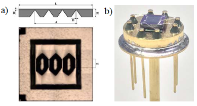
Fig: Design and layout of the glass-like carbon (GC)-based sensor:
a.) Schematic drawing of the GC strain sensor, and
b.) Enlarged optical microscopic image of a fabricated GC piezoresistor

Acknowledgements: The authors thank the Center of Micro/Nanotechnology (CMi) of EPFL for the microelectromechanical system (MEMS) fabrication support and Bio-Micro Robotics laboratory with Professor Hongsoo Choi of DGIST for the microforce probe system facility support. This work received funding from the European Research Council (ERC) under the European Union’s Horizon 2020 research and innovation program (Project “MEMS 4.0”, ERC-2016-ADG, Grant Agreement No. 742683) and the National Research Foundation of Korea (NRF) grant funded by the Korean government (MSIT) (No. 2020R1F1A107422211).

Feb 10, 2022

#SiC #CMOS Technology for High Temperatures


from Twitter https://twitter.com/wladek60

February 10, 2022 at 12:55PM
via IFTTT

#Analog #IC #design #Hackathon Digital India


from Twitter https://twitter.com/wladek60

February 10, 2022 at 12:52PM
via IFTTT

[paper] Special Topic on Materials and Devices for 5G Electronics

Nathan D. Orloff1, Rick Ubic2, and Michael Lanagan3
Special topic on materials and devices for 5G electronics
Appl. Phys. Lett. 120, 060402 (2022); 
DOI: 10.1063/5.0079175
1 NIST, Colorado, USA
2 Boise State University, Idaho, USA
3 Penn State University, Pennsylvania, USA

Abstract: Next generation communications are inspiring entirely new applications in education, healthcare, and transportation. These applications are only possible because of improvements in latency, data rates, and connectivity in the latest generation. Behind these improvements are new materials and devices that operate at much higher frequencies than ever before, a trend that is likely to continue. Beyond these exciting applications, higher frequency millimeter waves (mmWaves) may also address a growing problem with capacity. Today, most capacity problems occur when large numbers of wireless connections or applications access the network at the same time at any single location. As wireless internet connections far surpass wired connections and wireless data usage has grown exponentially for more than 10 years,3 many believe that capacity problems will spread without access to new bandwidth.

FIG: A plot of the peak data rates vs the operating frequency 
where the diameter of the circle is the bandwidth.

Acknowledgement: Our [the editors] special thanks to Lesley Cohen, Editor-in-Chief, Susan Trolier-McKinstry, Associate Editor, and Jessica Trudeau and Emma Nicholson Van Burns for their technical assistance with publishing.


Feb 9, 2022

[paper] SPICE simulation of PIN diodes and IGBT devices

Manhong Zhang, Yi Zhai
Recovering the carrier number conservation in SPICE simulation of PIN diodes and IGBT devices
Solid-State Electronics
Available online 7 February 2022, 108239
DOI: 10.1016/j.sse.2022.108239
   
North China Electric Power University, Beijing 102206, China


Abstract: In SPICE simulations of PIN diodes and IGBT devices using finite difference method, one discretizes an undepleted N- region into several equally spaced nodes with a time-dependent distance of Δx(t). Then transforms the ambipolar diffusion equation, a time-space partial differential equation, into a set of time-dependent ordinary differential equations. However, the time-dependent property of Δx(t) destroys the carrier number conservation. In this paper, we propose an approach to account for the effect of the Δx(t) by introducing an auxiliary system. It has the same total current and the total carrier number in the undepleted N- region as the real system, but has different electron and hole current components. The difference is caused by adding compensation current terms with the equal amplitude and opposite sign to the electron and hole current terms in the auxiliary system. These compensation current terms are proportional to the boundary speed of the undepleted N- region and do not change the total current. The auxiliary system can be easily solved using SPICE behavior models and its carrier density is a good approximation to the real one. Our simulations show that the compensation current correction is important for fast switching PIN diodes, but may not be very important in IGBT devices due to their large gate-related capacitance.
FIG: SPICE simulation model of PIN diodes and IGBT devices

[book] Nano Interconnects: Device Physics, Modeling and Simulation

Afreen Khursheed and Kavita Khare
Nano Interconnects: Device Physics, Modeling and Simulation
CRC Press; 1st edition (2021)
ISBN: ‎ 978-0367610487

This textbook comprehensively covers on-chip interconnect dimension and application of carbon nanomaterials for modeling VLSI interconnect and buffer circuits. It provides analysis of ultra-low power high speed nano-interconnects based on different facets such as material modeling, circuit modeling and the adoption of repeater insertion strategies and measurement techniques. It covers important topics including on-chip interconnects, interconnect modeling, electrical impedance modeling of on-chip interconnects, modeling of repeater buffer and variability analysis. Pedagogical features including solved problems and unsolved exercises are interspersed throughout the text for better understanding. Aimed at senior undergraduate and graduate students in the field of electrical engineering, electronics and communications engineering for courses on Advanced VLSI Interconnects, Advanced VLSI Design, VLSI Interconnects, VLSI Design Automation and Techniques, this book:

  • Provides comprehensive coverage of fundamental concepts related to nanotube transistors and interconnects.
  • Discusses properties and performance of practical nanotube devices and related applications.
  • Covers physical and electrical phenomena of carbon nanotubes, as well as applications enabled by this nanotechnology.
  • Discusses the structure, properties, and characteristics of graphene-based on-chip interconnect.
  • Examines interconnect power and interconnect delay issues arising due to downscaling of device size.

Feb 8, 2022

[App Note] Frenetic use A.I. technology to design optimal transformers

Frenetic is a power electronics company created with the goal of making magnetics simple. Frenetic is revolutionizing the world of magnetics with A.I. technology, which is replacing the need for outdated engineering methods. The A.I. technology allows designing optimal transformers and inductors, build and test samples in our laboratory and get the best manufacturing solutions for our clients in order to ensure that quality and timelines are respected.

App Note: Planar Transformer with Half Turns

New proposed solution for the transformer was based on a 4-column structure, where the flux cancellations reduce the core losses and allow keeping high power density. The solution was used in an LLC converter, obtaining a power density of 55 W/cm3.

References
[1] Y. -C. Liu et al., "Design and Implementation of a Planar Transformer With Fractional Turns for High Power Density LLC Resonant Converters," in IEEE Transactions on Power Electronics, vol. 36, no. 5, pp. 5191-5203, May 2021, doi: 10.1109/TPEL.2020.3029001.
[2] D. Huang, S. Ji and F. C. Lee, "LLC resonant converter with matrix transformer", IEEE Trans. Power Electron., vol. 29, no. 8, pp. 4339-4347, Aug. 2014.
[3] C. Fei, F. C. Lee and Q. Li, "High-efficiency high-power-density LLC converter with an integrated planar matrix transformer for high-output current applications", IEEE Trans. Ind. Electron., vol. 64, no. 11, pp. 9072-9082, Nov. 2017.

[paper] Atomic-scale defects in Si/SiO2 transistors

Stephen J. Moxim1, Fedor V. Sharov1, David R. Hughart2, Gaddi S. Haase2, Colin G. McKay2, and Patrick M. Lenahan1
Atomic-scale defects generated in the early/intermediate stages of dielectric breakdown in Si/SiO2 transistors
Appl. Phys. Lett. 120, 063502 (2022);
DOI:10.1063/5.0077946
   
1 The Pennsylvania State University, USA
2 Sandia National Laboratories, New Mexico, USA


Abstract: Electrically detected magnetic resonance and near-zero-field magnetoresistance measurements were used to study atomic-scale traps generated during high-field gate stressing in Si/SiO2 MOSFETs. The defects observed are almost certainly important to time-dependent dielectric breakdown. The measurements were made with spin-dependent recombination current involving defects at and near the Si/SiO2 boundary. The interface traps observed are Pb0 and Pb1 centers, which are silicon dangling bond defects. The ratio of Pb0/Pb1 is dependent on the gate stressing polarity. Electrically detected magnetic resonance measurements also reveal generation of E′ oxide defects near the Si/SiO2 interface. Near-zero-field magnetoresistance measurements made throughout stressing reveal that the local hyperfine environment of the interface traps changes with stressing time; these changes are almost certainly due to the redistribution of hydrogen near the interface.

FIG: Atomic-scale picture of defect formation and hydrogen motion during the early and intermediate stages of SiO2 degradation and breakdown.

Acknowledgements: This work was supported by the Defense Threat Reduction Agency (DTRA) under Award No. HDTRA1-18-0012. The content of the information does not necessarily reflect the position or the policy of the federal government and no official endorsement should be inferred

Feb 3, 2022

Aramco partners with Japan’s Yokogawa to localize chip manufacturing in Saudi Arabia


from Twitter https://twitter.com/wladek60

February 03, 2022 at 05:35PM
via IFTTT

[ESSDERC/ESSCIRC 2022] Call for Papers

Paper submission is open!
Submission deadline: Apr 12, 2022 23:59 (GMT -0700)
Decision notification: May 31, 2022 23:59 (GMT -0700)

The aim of ESSCIRC and ESSDERC is to provide an annual European forum for the presentation and discussion of recent advances in solid-state devices and circuits. The level of integration for system-on- chip design is rapidly increasing. This is made available by advances in semiconductor technology. Therefore, more than ever before, a deeper interaction among technologists, device experts, IC designers and system designers is necessary. While keeping separate Technical Program Committees, ESSCIRC and ESSDERC are governed by a common Steering Committee and share Plenary Keynote Presentations and Joint Sessions bridging both communities. Attendees registered for either conference are encouraged to attend any of the scheduled parallel sessions, regardless to which conference they belong.

PAPER SUBMISSION
Manuscript guidelines as well as instructions on how to submit electronically will be available on this website. Papers must not exceed four A4 pages with all illustrations and references included.
THE PAPERS SUBMISSION DEADLINE: APRIL 12, 2022

Papers submitted for review must clearly state:
•The purpose of the work
•How and to what extent it advances the state-of-the art
•Specific results and their impact

Only work that has not been previously published or submitted elsewhere will be considered. Submission of a paper for review and subsequent acceptance is considered as a commitment that the work will not be publicly available prior to the conference. After selection of papers, the authors will be informed about the decision of the Technical Program Committee by e-mail by 31 May 2022.

At the same time, the complete program will be published on the conference website. A binary feedback (accepted/rejected) with no comments will be provided to the authors. An oral presentation will be given at the Conference for each accepted paper. No-shows will result in the exclusion of the papers from any conference related publication. The submitted final PDF files should be IEEE Xplore compliant.

[paper] Transistor Modelling for mm-Wave Technology Pathfinding

B.Parvais1, R. ElKashlan1, H. Yu, A. Sibaja-Hernandez, B. Vermeersch, V. Putcha, P. Cardinael2, R. Rodriguez, A. Khaled, A. Alian, U. Peralagu, M. Zhao, S.Yadav, G. Gramegna, J. Van Driessche, N. Collaert
Transistor Modelling for mm-Wave Technology Pathfinding
SISPAD, 2021 
DOI: 10.1109/SISPAD54002.2021.959253
   
* imec, Kapeldreef 75, 3001 Leuven, Belgium
1 also with Vrije Universiteit Brussels, 1050 Brussels, Belgium
2 also with UCLouvain, Louvain-la-Neuve, Belgium


Abstract: A review of the modelling requirements to establish a Design-Technology Co-Optimization loop for mmWave Front-End Modules is presented. The example of GaN/Si technology is detailed, and recent modeling developments are explained.

Fig: The RF-DTCO loop concept: from device modeling
and exploration to benchmark circuits.


[paper] Piezosensitive Pressure Sensor Chip

Mikhail Basov
Pressure sensor chip utilizing electrical circuit of piezosensitive differential amplifier with negative feedback loop (PDA-NFL) for 5 kPa
XI International Scientific and Technical Conference 
"Micro-, and Nanotechnology in Electronics", 
Elbrus, Russia; June 2021
  
Dukhov Automatics Research Institute VNIIA, Moscow

Abstract: High sensitive (S=11.2±1.8 mV/V/kPa with nonlinearity error 2KNL=0.15±0.09 % /FS) small-sized (4.00x4.00 mm2) silicon pressure sensor chip utilizing new electrical circuit for microelectromechanical systems (MEMS) in the form of differential amplifier with negative feedback loop (PDA-NFL) for 5 kPa differential was developed. The advantages are demonstrated in the array of output characteristics, which prove the relevance of the presented development, relative to modern developments of pressure sensors with Wheatstone bridge electrical circuit for 5 kPa range.

Fig: a) Pressure sensor chip, b) its assembled structure


Feb 2, 2022

[EZMod3D] Comparing inductance extraction to measurement

EZMod3D is a division of EASii IC, which develops a 3D multi-domain physical simulation software solution (also called 3D field solver) mainly developed to process the design of integrated circuits (ASICs), printed circuit boards (PCBs) and both at the same time (CoDesign). EZMod3D was developed on the basis of an innovative solver enabling a fast simulation. This technology has allowed intensive use internally at EASii IC, targeting the requirements of R&D project: reducing iterations between design and manufacturing.

Very simple, you just need to start with your input data
  • GDS2 file, OASIS database, LEF / DEF (ASIC) or Gerber (PCB) or DXF (Packaging)
  • Technological file or materials description
  • The position of the potentials or flows to be applied
  • In pre-sizing step, you can sketchup using advanced user intergrated matrial library
FIG: An inductor, its 3D EZMod3D simulation and LCR measurements. EZMod3D now extracts inductance values and shows good agreement with measurements.
Measured value is 477nH; close to the simulated 481nH)

[paper] Modeling of SIC VDMOS FET

Anirban Kar∗, Ahtisham Pampori∗, Noriyoshi Hashimoto† and Yogesh Singh Chauhan∗
A Charge-Based Silicon Carbide MOSFET Compact Model for Power Electronics Applications
2021 IEEE 8th Uttar Pradesh Section UPCON)
DOI: 10.1109/UPCON52273.2021.9667643

∗Department of Electrical Engineering, IIT Kanpur (IN)
†Keysight Technologies (J)

Abstract: This paper presents a charge-based compact model for Silicon Carbide (SiC) power MOSFETs, which captures the static characteristics of the device over a wide range of voltages and currents. The drift region resistance and charges in the channel have been formulated to calculate the drain current in a self-consistent manner. The proposed model has been validated against the measured transfer and output characteristics of a commercial 1.2kV power MOSFET (Infineon IMW120R045M1) with a maximum current rating of 52A.

Fig: a) Transfer characteristics of SiC MOSFET with Vd=1 to 20V
b) Transconductance of SiC MOSFET with Vd=1 to 20V 

Acknowledgement: This work was supported in part by the Swarna Jayanti Fellowship under Grant DST/SJF/ETA02/2017-18 and in part by the Department of Science and Technology through the FIST Scheme under Grant SR/FST/ETII-072/2016 and Keysight Technologies, USA. The measurement of the device was carried out at Keysight Technologies, Japan.


Feb 1, 2022

IEEE SSCS PICO Contestants Cross the Finish Line

by Boris Murmann
DOI:10.1109/MSSC.2021.3135176
Date of current version: 24 January 2022

Last summer 2021, the IEEE Solid-State Circuits Society (SSCS) launched its first open source chip design contest under the umbrella of its Platform for Integrated Circuit Design Outreach program (PICO). Beginning with 61 submissions, a volunteer jury selected 18 teams from nine countries to embark on a journey toward tapeout. Anyone interested in supporting future activities is encouraged to sign up at the Society’s volunteer web portal. Stay tuned for the 2022 edition of the SSCS PICO contest!
FIG: Layout views of the chips submitted for tape out

      TABLE: A Summary Oof Designs Submitted for TapeOut
FunctionTeamChip URL
15G bidirectional amplifierPakistan 3 (National University of Computer and Emerging Sciences)https://efabless.com/projects/560
2Wireless power transfer unitPakistan 2 (National University of Computer and Emerging Sciences)
3Variable precision fused multiply–add unitPakistan 1 (National University of Computer and Emerging Sciences)
4Oscillator-based LVDT readoutIndia 2 (Anna University)https://efabless.com/projects/474
5Temperature sensorIndia 1 (Anna University)
6GPS baseband engineIndia 3 (Anna University)
7Ultralow-power analog front end for bio signalsBrazil 2 (Universidade Federal de Santa Catarina)https://efabless.com/projects/476
8TIA for quantum photonics interfaceUSA 4 (University of Virginia)https://efabless.com/projects/470
9Bandgap referenceEgypt (Cairo University)https://efabless.com/projects/473
10Neural network for sleep apnea detectionUSA 2 (University of Missouri)
11Sonar processing unitChile (University of the Bío-Bío)https://efabless.com/projects/54

Jan 31, 2022

[Google Research] Releases Circuit Training, an Open-Source Framework for Automated Chip Floorplanning #semi https://t.co/BD4iXWv5aS


from Twitter https://twitter.com/wladek60

January 31, 2022 at 05:48PM
via IFTTT