Showing posts with label chip. Show all posts

Jan 20, 2025

[book] From Code to Chip

Jakob Ratschenberger and Harald Pretl
From Code to Chip:
Open-Source Automated Analog Layout Design
pp: XV, 120 Publisher: Springer Cham (10 January 2025)
eBook ISBN 978-3-031-68562-0

This book shows how the layout of an analog circuit can be automatically generated in a fully open-source way. Based on an exemplary design flow, it introduces and explains the necessary steps for transforming a SPICE netlist into a layout, which can be inspected by the open-source layout editor Magic VLSI. This is done by using the industry’s first open-source process design kit SKY130. Furthermore, the implementation of the design flow in the programming language Python is available as open-source on GitHub. 

Authors' Affiliations
Johannes Kepler University, Linz, Austria


Table of contents (8 chapters)
  • Front Matter pp. i-xv
  • Download chapter PDF 
  • Introduction pp. 1-4
  • Theoretical Basics pp. 5-13
  • Circuit Capturing pp. 15-36
  • PDK—Design Rule Capturing pp. 37-41
  • Placement pp. 43-55
  • Routing pp. 57-71
  • Experimental Results pp. 73-99
  • Outlook pp. 101-103
  • Back Matter pp. 105-120


May 10, 2024

OSOC Initiative

Participators: Frontier System Laboratory, Architecture Laboratory
Status: Ongoing


The OSOC project guides students to design a tape-out open-source processor by combing EE with CS. It can help students improve their capacity of implementing software and hardware systems and learn how to design chips. Meanwhile, the project trains talents to be transferred to the high-performance processor "Xiangshan", open source EDA, open source IP and other teams and communities, which will continue to cultivate excellent reserve forces for advanced research and development of CS in China.

REF:
Institute of Computing Technology, Chinese Academy of Science 
No.6 Kexueyuan South Road Zhongguancun, Haidian District Beijing,China 
<https://acs.ict.ac.cn/english/projects_acs_en/202209/t20220927_46170.html>

Apr 30, 2024

[Kick-off] Chipdesign Germany

Chipdesign Germany
Das Netzwerk für Chipdesign in Deutschland
https://www.chipdesign-germany.de/
OnLine Registrierung: https://eveeno.com/auftaktchipdesigngermany

Juni 6. Donnerstag
13:00 Ankunft & Registrierung
14:00 Eröffnung
14:00 Begrüßung
Holger Blume; Leibniz Universität Hannover & edacentrum e.V.
14:15 Grußworte
Apollonia Pane Bundesministerium für Bildung und Forschung 
14:30 Vorstellung Chipdesign Germany
Holger Blume; Leibniz Universität Hannover & edacentrum e.V.
Norbert Wehn; Rheinland-Pfälzische Technische Universität Kaiserslautern-Landau
14:45 Keynote-Session I
14:45 Open-Source EDA and Innovation Leadership
Andrew B. Kahng; University of California San Diego, US
15:45 Kaffeepause
16:30 Keynote-Session II
16:30 Open Source Chip Design: Europas Weg zur Wettbewerbsfähigkeit in einer geteilten Tech-Welt?
Jan-Peter Kleinhans; Stiftung Neue Verantwortung
17:30 Mikroelektronik in digitalen Hörhilfen: Chips, die hören helfen
Joachim Thiemann; Advanced Bionic
18:30 Networking-Veranstaltung mit Poster- & Demo-Session

Juni 7. Freitag
08:30 Eröffnung
08:30 Begrüßung
Holger Blume; Leibniz Universität Hannover & edacentrum e.V
08:45 Keynote-Session III
08:45 Neue Fertigungstechnik für die Chipverarbeitung
Lutz Rissing; Dr. Johannes Heidenhain GmbH
09:45 Kaffeepause
10:30 DE:Sign Präsentationen
BMBF-Förderlinie "Design-Instrumente für souveräne Chipentwicklung mit Open-Source (DE:Sign)"
10:30 DI-OCRCpro
Daniel Krupka; Gesellschaft für Informatik e.V.
10:45 DI-DEMICO
Frank Ellinger; Technische Universität Dresden
11:00 DI-DERAMSys
Matthias Jung; Julius-Maximilian-Universität Würzburg
11:15 DI-OWAS
Dirk Koch; Ruprecht-Karls-Universität Heidelberg
11:30 DI-PASSIONATE
Robert Weigel; Friedrich-Alexander Universität Erlangen-Nürnberg
11:45 Interaktive Poster-Session
13:30 Verabschiedung

Adresse: Königlicher Pferdestall - Leibniz Universität Hannover; Appelstr. 7, 30167 Hannover
OnLine Registrierung: https://eveeno.com/auftaktchipdesigngermany


Mar 28, 2024

[paper] Chip Placement with Deep Learning

Azalia Mirhoseini, Anna Goldie, Mustafa Yazgan, Joe Jiang, Ebrahim Songhori, Shen Wang, Young-Joon Lee, Eric Johnson, Omkar Pathak, Sungmin Bae Azade, Nazi Jiwoo, Pak Andy, Tong Kavya Srinivasa, William Hang, Emre Tuncer, Anand Babu Quoc, Le James Laudon, Richard Ho, Roger Carpenter, Jeff Dean
Chip placement with deep reinforcement learning
arXiv preprint:2004.10746 (2020)

Abstract: In this work, we present a learning-based approach to chip placement, one of the most complex and time-consuming stages of the chip design process. Unlike prior methods, our approach has the ability to learn from past experience and improve over time. In particular, as we train over a greater number of chip blocks, our method becomes better at rapidly generating optimized placements for previously unseen chip blocks. To achieve these results, we pose placement as a Reinforcement Learning (RL) problem and train an agent to place the nodes of a chip netlist onto a chip canvas. To enable our RL policy to generalize to unseen blocks, we ground representation learning in the supervised task of predicting placement quality. By designing a neural architecture that can accurately predict reward across a wide variety of netlists and their placements, we are able to generate rich feature embeddings of the input netlists. We then use this architecture as the encoder of our policy and value networks to enable transfer learning. Our objective is to minimize PPA (power, performance, and area), and we show that, in under 6 hours, our method can generate placements that are superhuman or comparable on modern accelerator netlists, whereas existing baselines require human experts in the loop and take several weeks.

Fig: Visualization of placements. On the left, zero-shot placements from the pre-trained policy and on the right, placements from the finetuned policy are shown. The zero-shot policy placements are generated at inference time on a previously unseen chip. The pre-trained policy network (with no fine-tuning) places the standard cells in the center of the canvas surrounded by macros, which is already quite close to the optimal arrangement and in line with the intuitions of physical design experts.

Acknowledgments: This project was a collaboration between Google Research and the Google Chip Implementation and Infrastructure (CI2) Team. We would like to thank Cliff Young, Ed Chi, Chip Stratakos, Sudip Roy, Amir Yazdanbakhsh, Nathan Myung-Chul Kim, Sachin Agarwal, Bin Li, Martin Abadi, Amir Salek, Samy Bengio, and David Patterson for their help and support.


Nov 2, 2023

[paper] ChipNeMo

Mingjie Liu, Teo Ene, Robert Kirby, Chris Cheng, Nathaniel Pinckney, Rongjian LiangJonah Alben, Himyanshu Anand, Sanmitra Banerjee, Ismet Bayraktaroglu, Bonita Bhaskaran Bryan Catanzaro, Arjun Chaudhuri, Sharon Clay, Bill Dally, Laura Dang, Parikshit Deshpande Siddhanth Dhodhi, Sameer Halepete, Eric Hill, Jiashang Hu, Sumit Jain, Brucek Khailany Kishor Kunal, Xiaowei Li, Hao Liu, Stuart Oberman, Sujeet Omar, Sreedhar Pratty, Ambar Sarkar Zhengjiang Shao, Hanfei Sun, Pratik P Suthar, Varun Tej, Kaizhe Xu, Haoxing Ren
ChipNeMo: Domain-Adapted LLMs for Chip Design
arXiv:2311.00176 [cs.CL]
DOI: 10.48550/arXiv.2311.00176

* NVIDIA

Abstract: ChipNeMo aims to explore the applications of large language models (LLMs) for industrial chip design. Instead of directly deploying off-the-shelf commercial or open-source LLMs, we instead adopt the following domain adaptation techniques: custom tokenizers, domain-adaptive continued pretraining, supervised fine-tuning (SFT) with domain-specific instructions, and domain-adapted retrieval models. We evaluate these methods on three selected LLM applications for chip design: an engineering assistant chatbot, EDA script generation, and bug summarization and analysis. Our results show that these domain adaptation techniques enable significant LLM performance improvements over general-purpose base models across the three evaluated applications, enabling up to 5x model size reduction with similar or better performance on a range of design tasks. Our findings also indicate that there’s still room for improvement between our current results and ideal outcomes. We believe that further investigation of domain-adapted LLM approaches will help close this gap in the future.
Fig: LLM script generator integration with EDA tools

Acknowledgements: The authors would like to thank: NVIDIA IT teams for their support on NVBugs integration; NVIDIA Hardware Security team for their support on security issues; NVIDIA NeMo teams for their support and guidance on training and inference of ChipNeMo models; NVIDIA Infrastructure teams for supporting the GPU training and inference resources for the project; NVIDIA Hardware design teams for their support and insight.

Feb 3, 2022

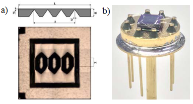
[paper] Piezosensitive Pressure Sensor Chip

Mikhail Basov
Pressure sensor chip utilizing electrical circuit of piezosensitive differential amplifier with negative feedback loop (PDA-NFL) for 5 kPa
XI International Scientific and Technical Conference 
"Micro-, and Nanotechnology in Electronics", 
Elbrus, Russia; June 2021
  
Dukhov Automatics Research Institute VNIIA, Moscow

Abstract: High sensitive (S=11.2±1.8 mV/V/kPa with nonlinearity error 2KNL=0.15±0.09 % /FS) small-sized (4.00x4.00 mm2) silicon pressure sensor chip utilizing new electrical circuit for microelectromechanical systems (MEMS) in the form of differential amplifier with negative feedback loop (PDA-NFL) for 5 kPa differential was developed. The advantages are demonstrated in the array of output characteristics, which prove the relevance of the presented development, relative to modern developments of pressure sensors with Wheatstone bridge electrical circuit for 5 kPa range.

Fig: a) Pressure sensor chip, b) its assembled structure


Feb 21, 2017

1-cent "lab on a chip" could save lives

Rahim Esfandyarpour, Stanford University, helped to develop a way to create a diagnostic "lab on a chip" for just a penny:
"I'm pretty sure it will open a window for researchers because it makes life much easier for them - just print it and use it," said Esfandyarpour. The results of this research were recently published in the journal Proceedings of the National Academy of Sciences [Source: Stanford Medicine]