Feb 18, 2026
[paper] Compact Modeling of Ferroelectric Devices
Jan 16, 2026
2026 Asia-Pacific Workshop on Advanced Semiconductor Devices
AWAD 2026 Venue
Asti Hotel Busan Important Dates Paper submission deadline: Apr 19, 2026 Acceptance notification: May , 2026 Author registration: June, 2026 Advance registration: June, 2026 |
Topics of Interest
|
- The Institute of Electronics and Information Engineers (IEIE), Korea
- The Institute of Electronics, Information and Communication Engineers (IEICE-ES), Japan
- IEEE Electron Devices Society (EDS) Seoul Section Chapter
Apr 25, 2024
[PhD] Transient Simulation of Frequency Domain Devices in Gnucap
Apr 3, 2024
[Overview] Radiation Damage Effects in Microelectronic Devices
and Longxian Li1
1 Naval University of Engineering, Wuhan 430033, China
2 PLA Unit 91049, Sanya 572000, China
Abstract: With the rapid advancement of information technology, microelectronic devices have found widespread applications in critical sectors such as nuclear power plants, aerospace equipment, and satellites. However, these devices are frequently exposed to diverse radiation environments, presenting significant challenges in mitigating radiation-induced damage. Hence, this review aims to delve into the intricate damage mechanisms of microelectronic devices within various radiation environments and highlight the latest advancements in radiation-hardening techniques. The ultimate goal is to bolster the reliability and stability of these devices under extreme conditions. The review initiates by outlining the spectrum of radiation environments that microelectronic devices may confront, encompassing space radiation, nuclear explosion radiation, laboratory radiation, and process radiation. It also delineates the potential damage types that these environments can inflict upon microelectronic devices. Furthermore, the review elaborates on the underlying mechanisms through which different radiation environments impact the performance of microelectronic devices, which includes a detailed analysis of the characteristics and fundamental mechanisms of damage when microelectronic devices are subjected to total ionizing dose effects and single-event effects. In addition, the review delves into the promising application prospects of several key radiation-hardening techniques for enhancing the radiation tolerance of microelectronic devices.
Nov 1, 2023
IWPSD 2023
- 2D Materials and Devices
- Crystal Growth and Epitaxy
- Device Modelling and Simulation
- Devices for Quantum Technology
- II - VI and Oxide Semiconductors
- III - V Semiconductors
- Memory and Logic Devices
- MEMS, NEMS and Sensors
- Organic and Flexible Electronics
- Photovoltaics
- Power Semiconductor Devices
- Optoelectronics
Sep 29, 2023
[workshop] QC:DCEP 2023
plus additional technical talks
Sep 10, 2023
[book] Advanced Ultra Low-Power Semiconductor Devices
Edited by Shubham Tayal, Abhishek Kumar Upadhyay, Shiromani Balmukund Rahi, and Young Suh Song
ISBN: 9781394166411 | (C)2023 Hardcover | 306 pages
Sep 5, 2023
[C4P] EDTM Conference 2024, Bangalore
Advances in modeling/simulation of devices, packages and processes; Technology CAD and benchmarking; Atomistic process and device simulation; Compact models for DTCO and STCO; AI/ML-augmented modelling; Material and interconnect modeling; Models for photonic devices.
- Three-page camera-ready paper submission starts: August 1,2023
- Paper submission deadline:
October 15, 2023October 30, 2023 - Notification for Acceptance: December 15, 2023
Accepted IEEE EDTM 2024 papers will be considered for competition for the Best Paper Award, Best Student Paper Awards and Best Poster Awards.
More details on paper submission can be found at the Paper Submission webpage.
Sep 4, 2023
[Proceedings] MNDCS 2023
Jan 19, 2023
IEEE EDS MQ at NIT Silchar Silchar, Assam (IN)
| DATES | LOCATION | HOST | REGISTER |
|---|---|---|---|
| Date: 29 Jan 2023
Time:10:00AM to 06:00PM (UTC+05:30) Add Event to Calendar | National Institute of Technology Silchar
Dept of ECE, NIT Silchar Silchar, Assam India 788010 Building: ECE/CSE Building | National Inst of Technology - Silchar, ED15 Kolkata Section Chapter NANO42 Co-sponsored by Dr. Trupti R. Lenka | Starts Dec.1, 2022 Ends Jan.28,2023 No Admission Charge Register NOW |
- Anil Kottantharayil (anilkg@ieee.org)
- Gananath Dash (gndash@ieee.org)
- Ajit Kumar Panda (akpanda62@hotmail.com)
- Manoj Saxena (msaxena@ieee.org)
- Brajesh Kumar Kaushik (bkkaushik23@gmail.com)
- Samar Saha (samar@ieee.org)
- Hiroshi Iwai (h.iwai@ieee.org)
- Taiichi Otsuji (taiichi.otsuji.e8@tohoku.ac.jp)
- Pei-Wen Li (pwli@nycu.edu.tw)
- Zhou Xing (EXZHOU@ntu.edu.sg)
- Albert Chin (albert_achin@hotmail.com)
- Mansun Chan (mchan@ust.hk)
- Chao-Sung LAI (cslai@mail.cgu.edu.tw)
- Wladek Grabinski, MOS-AK, EU (wladek@grabinski.ch)
Jan 17, 2023
UPCOMING – Winter School in III-Sb applications
- Prof. Dr. Manus Hayne, Lancaster University Birth of the ULTRARAM TM Concept
- Prof. Dr. Dieter Bimberg, Technische Universität Berlin Quantum Dot-Based Flash Memories: The Holy Grail at Sunrise?
- Dr. Petr Klenovský, Masaryk University, Brno Modeling Electronic states of IlI-Sb guantum systems on GaP substrate
- Dr. Wladek Grabinski, MOS-AK (EU) FOSS TCAD/EDA Tools for Compact Modeling
- Prof. Vihar Georgiev, James Watt School of Engineering, Glasgow Nano-electronic Simulation Software (NESS): a flexible nano-device simulation platform
- PD Dr. Uwe Bandelow, WIAS Berlin TBA
- Prof. Claudia Dr.axl, Humboldt Universität Berlin Unsupervised learning for insight into high-throughput calculations
- Rabea Pons, Comsol, Göttingen Introduction into COMSOL and hands-on session
- Prof. Dr. Mathieu Luisier, ETH Zürich TBA
- Dr. Marc Bescond, Faculté des Sciences de Saint Jérôme, NQS group, Marseille TBA
- Dr. Chetan Gupta, Micron Technology (R&D) Industry perspective on memory technologies
- Prof. Dr. Jannik Wolters, Deutschen Zentrum für Luft- und Raumfahrt / TU Berlin Quantum Memories and Introduction into Quantum Technologie
Sep 14, 2022
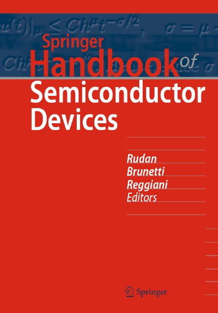
Handbook of Semiconductor Devices
- Covers physical backgrounds, fabrication, application and modeling
- Describes in detail both conventional and innovative devices
- An indispensable resource for practitioners, professionals and researchers
Basic devices and applications
New-generation devices and architectures
Modeling
Feb 10, 2022
[paper] Special Topic on Materials and Devices for 5G Electronics
2 Boise State University, Idaho, USA
3 Penn State University, Pennsylvania, USA
Jun 28, 2021
Program 2021: Symposium on Schottky Barrier MOS Devices
The symposium goal is to combine the activities of an enthusiastic group of Schottky barrier researchers worldwide. The topics cover all important aspects of potential applications, simulation and modeling, processing and implementation for CMOS/SOI technologies, Quantum technologies and approaches for neuromorphic applications. The content will be beneficial for anyone who needs to learn the opportunities and challenges of this technology since the first introduction by Walter Schottky in the 1938s. New aspects and future proposals to make the Schottky barrier into the main stream are welcome.
| Wed 30.06.2021 (Virtual) |
|---|
| 13:00-13:05 | Opening IEEE DL |
| 13:05-14:00 | IEEE Distinguished Lecture: Tunneling Graphene FET Gana Nath Dash, Sambalpur University (IN) Abstract: During the last few decades, aggressive scaling in Si MOSFET (Metal Oxide Semiconductor Field Effect Transistor) architecture has given rise to several short channel effects, which in turn has set a performance limit on the device owing to constraint in Si technology. The emergence of graphene at this juncture with a host of exotic and favorable electronic properties, generated new hopes for the FET industry. While the graphene based analogue FET witnessed some advantages, the digital counterpart showed a dismal performance, primarily due to the zero bandgap of graphene (poor ON/OFF ratio). For a way out, an alternative architecture based on the quantum tunneling process is augmented with the graphene FET resulting in the new device named TGFET. |
| 14:00-14:05 | Opening SSBMOS |
| 14:05-14:35 | Germanium nanosheet and nanowire transistor technologies for beyond CMOS applications Walter M. Weber, Raphael Böckle, Lukas Wind, Kilian Eysin, Daniele Nazzari, Tatli Ezgi, Oliver Solfronk, Alois Lugstein and Masiar Sistani, Institute of Solid State Electronics, TU Vienna (A) Abstract: The ultimate downscaling limits of conventional field effect transistors calls for alternative computational methods that provide perspectives towards the enhancement of computational complexity, circuit performance and energy efficiency. In this sense germanium nano-transistors offer both an approachable access to quantum confinement effects and promising electronic transport properties that distinctly are compatible with modern CMOS fabrication flows. We will discuss the applicability of different germanium active regions and gating architectures towards the realization of computational electronics with added functionality. On top of exploring different realizations of reconfigurable transistors with programmable polarity we will discuss further functionality enhancement by enabling operability within the negative differential resistance regime at room temperature. Prospective implications at the circuit level will be discussed. |
| 14:40-15:10 | Evolving contact-controlled thin-film transistors Radu Sporea, University of Surrey (UK) Abstract: TFT designs that comprise multiple gates and rectifying source contacts can be designed to produce linear transconductance and act as robust amplifiers and signal converters. This talk outlines device design and opportunities in emerging edge processing applications. |
| 15:10-15:50 | COFFEE BREAK |
| 15:50-16:20 | Compact Modelling of Dually-Gated Reconfigurable Field-Effect Transistors Christian Römer*, Ghader Darbandy*, Mike Schwarz*, Jens Trommer**, André Heinzig**, Thomas Mikolajick**, Walter M. Weber***, Benjamín Iñíguez**** and Alexander Kloes* *NanoP, THM (DE), **namLAB, TU Dresden (DE), ***TU Vienna (A), ****DEEEA, URV (ES) Abstract: This work presents a closed-form and physics-based DC compact model, which is applicable on dually-gated reconfigurable field-effect transistors (RFETs). The presented compact model is focused on the charge-carrier injection at the device’s source and drain side Schottky barriers, which can be separated into field emission and thermionic emission current contributions. This work explains the basic equations which are used to calculate the current contributions and shows calculated device characteristics compared to measurements. |
| 16:25-16:55 | The Schottky barrier transistor in all its forms Laurie Calvet*, John P. Snyder**, Mike Schwarz*** *C2N, University Paris (FR),** JCap, LLC (USA), ***NanoP, THM (DE) Abstract: The Schottky barrier (SB) transistor, where the source and drain of a conventional planar MOSFET are replaced with metallic contacts, was first explored in the 1960s. Since then, many variations on this structure have been explored in the literature including: different semiconductors materials such as other non-organic semiconductors and nano-structures such as carbon nanotubes and nanowires. In this talk we review some of the changes in the electronic transport that are observed as the geometry and materials of the SB transistors are changed. |
May 6, 2021
[Workshop] The Future of Nanoelectronics Devices and Systems Beyond Moore

- Beyond CMOS and Emerging Materials
- Trends in Beyond CMOS
Clivia Sotomayor-Torres; ICN2 and Jouni Ahopelto; VTT - 2D semi-metal to semiconductor transition devices and/or doping of 2D materials
Farzan Gity; Tyndall - GeSn/Ge vertical nanowire GAA FETs
Qing-Tai Zhao; FZJ - Flexible electronics with 2D materials
Zhenxing Wang; AMO - Presentation of the new IRDS More than Moore Roadmap
Mart Graef; TU Delft - Energy Harvesting for Autonomous Systems
- Summary of the IRDS Energy Harvesting for Autonomous Systems White Paper
Gustavo Ardila; UGA - Energy sustainability problems of IoT networks
Thomas Skotnicki; CEZAMAT - Contribution of triboelectricity for kinetic energy harvesting using electrostatic transduction
Philippe BASSET; ESIEE, Paris - Smart Sensors
- Summary of the IRDS Smart Sensors White Paper
Alan O’Riordan; Tyndall - Sensing at the Edge: Challenges and Opportunities
Adrian Ionescu; EPFL - Smart Sensors and Systems for environment and human exposure monitoring
Carmen Moldovan; IMT - Smart Energy
- Summary of the IRDS Smart Energy White Paper
Mikael Ostling; KTH - Smart power devices based Wide Bandgap semiconductors
William Vandendaele; CEA LETI - Materials and substrates for future power devices
Joff Derluyn; Soitec BU EpiGaN - Flexible/Wearable Electronics
- Roadmap of Flexible Electronics: Challenges and Possible Solutions; Summary of the IRDS White Paper
Benjamin Iñiguez; URV - Schottky barrier and organic devices for neuromorphic circuits
Laurie Calvet; CNRS; Université Paris Saclay - New strategies for sustainable electronics
Elvira Fortunato; UNL
 |
 |
 |
Feb 11, 2021
[symposium] ISDCS 2021 Hiroshima University
- Prof. Parthasarathi Chakrabarti, Director, IIEST Shibpur and Department of Electronics Engineering, IIT(BHU), India
"Advanced Materials and Methods for Fabrication of Thin-film Transistor (TFT)-based Sensors" - Prof. Shinji Kaneko, Hiroshima University, Japan
"SDGs Initiatives at Hiroshima University: Integrating Global Strategy and Regional Vitalization"
- Prof. Sanatan Chattopadhyay, University of Calcutta, India
"Voltage Assisted Quantum Dot Based MOS Devices for Electronic and Optoelectronic Applications" - Prof. Partha Bhattacharya, IIEST Shibpur, India
"Performance Improvement of Graphene Derivative based Gas sensors: Role of Functional Group Tuning and Ternary Junction Formation" - Prof. Hafizur Rahaman, IIEST Shibpur, India
"Tunnel Field Effect Transistors: Challenges and Opportunities" - Prof. Nillohit Mukherjee, IIEST Shibpur, India
"Metal Oxide Semiconductors with Carbon Nanomaterials for Efficient Supercapacitive Type Energy Storage Devices" - Prof. Shigeyasu Uno, Ritsumeikan University, Japan
"Electrochemical Impedance Sensor for Non-invasive Living Cell Monitoring toward CMOS Cell Culture Monitoring Platform" - Mr. Shigeru Shiratake, Corporate Vice President, DRAM, Emerging Memory Process Integration and Device Technology Micron Technology, Inc., USA
"Challenges for DRAM scaling and performance enhancement" - Prof. Rihito Kuroda, Tohoku University, Japan
TBD
Previous Conference:
- ISDCS 2020, Kolkata, India
- ISDCS 2019, Higashi-hiroshima, Japan
- ISDCS 2018, Kolkata, India
Jan 17, 2021
Virtual Si Museum /2103/ Electron Devices Scaling
Other look at the electron device scaling: Trinitron CRT vs iPhone6 Retina HD LED display. Both were extracted for broken units:) Trinitron CRT (Sony's brand name for its line of aperture-grille-based CRTs) were introduced in 1968. Its standard TV resolution was 720x576-pixel for PAL. iPhone6 available since 2014 has the HD LED display 1334x750-pixel. Just estimate volume, resolution and power consumption scaling in both cases.
- Sony Trinitron A13JZVOOX
5-inch (diagonal) CRT 720x576-pixel resolution for PAL at 192 ppi - iPhone6 Retina HD display
4.7-inch (diagonal) LED 1334x750-pixel resolution at 326 ppi


