Jul 21, 2021

[paper] 11.8 GHz Fin Resonant Body Transistor

Analysis and Modeling of an 11.8 GHz Fin Resonant Body Transistor 
in a 14nm FinFET CMOS Process 
Udit Rawat, Student Member, IEEE, Bichoy Bahr*, Member, IEEE, 
and Dana Weinstein, Senior Member, IEEE
arXiv:2107.04502v1 [physics.app-ph] 9 Jul 2021
 
Department of Electrical Engineering, Purdue University, West Lafayette USA
*Kilby Labs - Texas Instruments, Dallas, TX, USA.

Abstract: In this work, a compact model is presented for a 14 nm CMOS-based FinFET Resonant Body Transistor (fRBT) operating at a frequency of 11.8 GHz and targeting RF frequency generation/filtering for next generation radio communication, clocking, and sensing applications. Analysis of the phononic dispersion characteristics of the device, which informs the model development, shows the presence of polarization exchange due to the periodic nature of the back-end-of-line (BEOL) metal PnC. An eigenfrequency-based extraction process, applicable to resonators based on electrostatic force transduction, has been used to model the resonance cavity. Augmented forms of the BSIM-CMG (Common Multi-Gate) model for FinFETs are used to model the drive and sense transistors in the fRBT. This model framework allows easy integration with the foundry-supplied process design kits (PDKs) and circuit simulators while being flexible towards change in transduction mechanisms and device architecture. Ultimately, the behaviour is validated against RF measured data for the fabricated fRBT device under different operating conditions, leading to the demonstration of the first complete model for this class of resonant device integrated seamlessly in the CMOS stack.
Fig: Complete 3D FEM Simulation model depicting two adjoining fRBT unit cells. Mx (x=1-3) and Cy (y=4-6) represent the first 6 metal levels that form a part of the BEOL PnC.

Acknowledgement: This work was supported in part by the DARPA MIDAS Program.


#MEMS becoming more #human


from Twitter https://twitter.com/wladek60

July 21, 2021 at 10:22AM
via IFTTT

Jul 17, 2021

VSD Free Webinar - Mixed-signal RISC-V based SoC on FPGA - 23rd July, 7pm IST


This 60-min webinar helps you get started with a basic mixed-signal FPGA flow, which can be extended to any complex SoC.VSD and RedwoodEDA conducts 5-day RISC-V based MYTH (Microprocessors for You in Thirty Hours) workshop using transaction level Verilog on Makerchip platform. For people who have done this workshop can use this webinar as an extension to the 5th Day, where RISC-V pipe-lined CPU coded in TL-Verilog is now converted to Verilog language and is a part of a mixed-signal SoC

If you are from ASIC/Physical design back-ground, this webinar will complement your existing work, and you would really get to know similarities and differences between ASIC and FPGA flow, which one is preferred under what conditions and why is it preferred

This single webinar connects VLSI students, analog designers, FPGA designers and ASIC designers. It is also an attempt to bring everyone on the same platform, and serves as a starting point for design verification

Stay tuned for follow-up series of FPGA webinars and 5-day hands-on high intensity FPGA workshop, which will be built around OpenFPGA framework and Makerchip visualization software, that enables the whole community to learn FPGA fundamentals along with labs, without actually having a physical FPGA board.

Agenda:
  1. "FPGA on eSim"
    Guest Speaker - Prof. Kannan M Moudgalya, IIT Bombay
  2. "chipIgnite Program"
    Guest Speaker - Mike Wishart, CEO eFabless
  3. "Tapeout World Program"
    Guest Speaker - Naveed Sherwani, Chairman, OSFPGA
  4. "Mixed-signal RISC-V based SoC on FPGA"
    Webinar Instructor - Shivani Shah

Webinar Curriculum:
1) Introduction
2) RVMYTH RISC-V Core
3) Why FPGAs ?
4) TL - Verilog to RTL verilog using Makerchip
5) Functional Simulation using iverilog
6) FPGA - Steps to create project
7) FPGA - Steps to generate IPs
8) FPGA - RTL simulation
9) FPGA - Synthesis
10) FPGA - Implementation and timing analysis
11) FPGA - Bit-stream generation, FPGA programming and ILA
12) Conclusion

Register here (if you don't see the form, please refresh page):
https://lnkd.in/gByg6fZ

Jul 15, 2021

[Announcement] ToM 2021/2 online on September 21st-23rd


ToM2021/2 course will be held online on September 21st-23rd, 2021 with the following program:
September 21 2021
    14:00 – 17:30 Jussi Jansson (Oulu University, Finland) - "Time-to-digital converters and related applications"
September 22 2021
    09:00 – 12:30 Luca Scandola (Infineon Technologies, Italy), "Introduction to DC-DC conversion suitable for automotive application: from the theory to the modelization with practical examples"
    14:00 – 17:30 Benoit Bakeroot (Ghent University, Belgium), "GaN semiconductor devices for power electronics: overview, status and future perspectives"
September 23 2021
    09.00 – 12:30 Qiang Li (UETSC, China), "Subthreshold and near-threshold ADC techniques"
    14:00 – 17:30 Andrea Mazzanti (University of Pavia, Italy) and Enrico Monaco (Inphi, Italy), "Introduction and advances in serial links"

=============================================

Registration is mandatory to attend the course:
http://www.innotechevents.com/index.php?page=ToM/RegistrationForm.html

Registered participants will receive:
- on-line attendance to all lectures
- pdf material for all lectures
- certificate of participation
- final exam with certificate (if needed)

We look forward to virtually meeting you !!!!

More information at:
http://www.innotechevents.com/index.php?page=ToM/ToM.html

Best regards
Andrea Baschirotto

#SiFive Technical Symposium // India and Bangladesh


from Twitter https://twitter.com/wladek60

July 15, 2021 at 11:41AM
via IFTTT

Jul 13, 2021

Last chance for IEEE Mauritius Conference


Dear colleagues,

Due to many requests, the paper submission deadline has been extended to 25th July 2021 ! This is last due date .

We are pleased to invite you to participate to the IEEE - International Conference on Electrical, Computer, Communications and Mechatronics Engineering (ICECCME) which will be held in Mauritius, the Paradise Island on 07-08 October, 2021. The ICECCME is the premier event that brings together industry professionals, academics, and engineers from the related institutions to exchange information and ideas on electrical, computer, communications and mechatronic engineering.

All accepted and presented papers will be submitted to IEEE Xplore for publication.

The extended versions of selected papers will be published in SCI-indexed Energies journal with IF: 2.702

Due to the Covid pandemic, ICECCME will be held both face-to-face and online. Participants can make their presentations online.

You can see all the details on the conference web page: http://www.iceccme.com

The conference will take place in Mauritius surrounded by the warm Indian Ocean.
Mauritius is one of the best holiday destinations in the world with clear warm sea waters, attractive beaches, tropical fauna and flora.

Come to Mauritius, reward yourself!

If you would like to be a reviewer...

You can review the papers from our conferences and journal. By acting as a reviewer, you can earn discounts on conference participation fees (from any of our conferences). In addition we will send reviewer certificate.
Click here to reviewer application

Important Dates:
Paper Due :  25 July, 2021
Acceptance Notification :  10 August, 2021
Early Registration Deadline:
15 August, 2021
Camera Ready Due : 20 August, 2021
Conference Dates: 7-8 October 2021

Best regards,
Conference Organizing Team

E-mail: info@iceccme.com  
Phone(Whatsapp): +90 532 6425237
Projenia R&D Co. Erciyes TGB, No:67/10 TR

Follow us on social media to be informed for our events.


If you do not want to receive mail from us anymore, please unsubscribe. 
When you unsubscribe from the list, definetely no e-mail will be sent to you after that.

[paper] ML based Aging-Aware FPGA Framework

Behnam Ghavami, Milad Ibrahimipour, Zhenman Fang, Lesley Shannon 
MAPLE: A Machine Learning based Aging-Aware FPGA Architecture Exploration Framework
31st International Conference on Field-Programmable Logic and Applications
(FPL 2021 Short Paper),
Virtual Conference, Sept 2021
*Simon Fraser University, Burnaby, BC, Canada

Abstract: In this paper, we develop a framework called MAPLE to enable the aging-aware FPGA architecture exploration. The core idea is to efficiently model the aging-induced delay degradation at the coarse-grained FPGA basic block level using deep neural networks (DNNs). For each type of the FPGA basic block such as LUT and DSP, we first characterize its accurate delay degradation via transistor-level SPICE simulation under a versatile set of aging factors from the FPGA fabric and in-field operation. Then we train one DNN model for each block type to quickly and accurately predict the complex relation between its delay degradation and comprehensive aging factors. Moreover, we integrate our DNN models into the widely used Verilog-to-Routing toolflow (VTR 8) to support analyzing the impact of aging-induced delay degradation on the entire large scale FPGA architecture. Experimental results demonstrate that MAPLE can predict the delay degradation of FPGA blocks 104 to 107 times faster than transistor-level SPICE simulation, with a prediction error less than 0.7%. Our case study demonstrates that FPGA architects can effectively leverage MAPLE to explore better aging-aware FPGA architectures.

Fig: Overview of FPGA fabric and in-field factors affecting FPGA aging at transistor and basic block levels. We use DNNs to model FPGA delay degradation at basic block level.

Acknowledgements: We acknowledge the support from Government of Canada Technology Demonstration Program and MDA Systems Ltd; NSERC Discovery Grant RGPIN-2019-04613 and DGECR 2019-00120; Canada Foundation for Innovation John R. Evans Leaders Fund; Simon Fraser University New Faculty Start-up Grant; Xilinx, Huawei and Nvidia.

SK hynix Starts Mass Production of #1anm DRAM


from Twitter https://twitter.com/wladek60

July 12, 2021 at 11:34PM
via IFTTT

From Garage to Tech Giant


from Twitter https://twitter.com/wladek60

July 12, 2021 at 11:38PM
via IFTTT

Jul 12, 2021

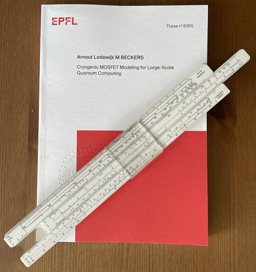
[PhD] Cryogenic MOSFET Modeling

Cryogenic MOSFET Modeling for Large-Scale Quantum Computing
Arnout Lodewijk M BECKERS
Thèse n° 8365 2021
DOI: 10.5075/epfl-thesis-8365

Présentée le 28 mai 2021

Faculté des sciences et techniques de l’ingénieur Laboratoire de circuits intégrés Programme doctoral en génie électrique

pour l’obtention du grade de Docteur ès Sciences par
Arnout Lodewijk M BECKERS

Acceptée sur proposition du jury:
Prof. E. Charbon, président du jury
Prof. C. Enz, directeur de thèse
Prof. B. Parvais, rapporteur
Prof. G. Ghibaudo, rapporteur
Dr J.-M. Sallese, rapporteur 

Abstract: Promising results of state-of-the-art quantum computers fuel a world-wide effort in academic and private research laboratories to scale up the number of qubits and improve their characteristics in large arrays. To meet the scale-up challenge, innovative microelectronic architectures are envisioned hosting qubits and transistors in silicon. Integrated-circuit design for deep-cryogenic temperatures (below 10 K or -263.15°C) is a challenging optimization exercise that currently leads to costly iterations due to the lack of physics-based transistor models for these temperatures. Proposed enhancements to the industry-standard transistor models neglect the low-temperature physics and do not suffice for a large-volume application. This PhD thesis pushes the state-of-the-art of the characterization, physics, and modeling of CMOS (Complementary Metal Oxide Semiconductor) transistors down to deep-cryogenic temperatures. The most advanced commercial bulk CMOS technology (28-nm minimum gate length) is measured down to 4.2 K using dip-stick measurements and probe-station measurements. The temperature behavior of the physical parameters and the analog figures-of-merit is reported. A similar characterization study is presented for a 28-nm FDSOI CMOS technology using measurements provided by CEA-Léti through the EU H2020 MOS-Quito Project. It is shown that the design methodology based on the transconductance efficiency remains valid down to 4.2 K for both advanced CMOS processes. These results are already supporting the community: qubit controllers in 28-nm bulk and FDSOI technologies have been successfully deployed in the cryostats of quantum computers by Google and CEA-Léti, respectively. Industry-standard models have been honed over many years for near room-temperature operation. They show the largest discrepancies in the sub- and near-threshold regimes when used at deep-cryogenic temperatures. Therefore, this thesis presents an in-depth study of these regimes. Generalized Boltzmann relations are derived including band tails, which are valid in subthreshold. Using these relations, a new analytical theory is derived for the subthreshold swing that rolls off from the Boltzmann limit, showing that an ideal step-like switch cannot be obtained in the 0-K limit due to shallow band-edge states. The process quality must be improved to operate devices closer to the Boltzmann limit. Moreover, the transconductance efficiency in weak inversion (subthreshold) follows the new theoretical limit instead of the Boltzmann temperature limit. This mitigates the expected current savings from biasing in weak inversion. The new theory also explains the impossible inverse temperature dependence of the subthreshold-slope factor, which has been extracted in numerous characterizations in the literature. Furthermore, a threshold-voltage model for bulk CMOS is presented including dopant freezeout and interface traps. Process engineers can benefit from this model to customize transistors for use at 4.2 K. Finally, the discrepancy of the transfer characteristics in moderate inversion (near-threshold) is modeled with an improved representation of the localized band-edge states. As such, this PhD thesis lays the groundwork for next-generation deep-cryogenic IC design benefiting from physics-based knowledge. While this thesis is oriented toward quantum computing, the results also apply to other deep-cryogenic applications at the forefront of science and engineering.
Fig: Different explanations have been proposed for the deviation of the subthreshold swing (SS) from the Boltzmann limit at deep-cryogenic temperatures (below a critical temperature Tc). This led to the introduction of band-edge states to explain SS(T)

How to double research citations?


https://www.psypost.org/2021/07/the-sci-hub-effect-can-almost-double-the-citations-of-research-articles-study-suggests-61425

[RsyPost] For their study, the researchers examined 8,661 scientific articles published in three multidisciplinary journals (Nature, Science, and Proceedings of the National Academy of Sciences), three economic journals (The Quarterly Journal of Economics, Journal of Political Economy, and Econometrica), three consumer research journals (Journal of Consumer Research, Journal of Retailing and Consumer Services, and Journal of Consumer Psychology), and three neuroscience journals (Nature Reviews Neuroscience, Nature Neuroscience, and Neuron).

The articles were published between September 2015 and February 2016. About half of them had been downloaded from Sci-Hub, while the other half had never been downloaded from the website.


PsyPost is an independently-owned psychology and neuroscience news website dedicated to reporting the latest research on human behavior, cognition, and society. The publication covers the latest discoveries in psychology, psychiatry, neuroscience, sociology, and similar fields.


Jul 9, 2021

#OpenPOWER Foundation | #Libre-SOC #180nm Power ISA ASIC Submitted to Imec for Fabrication https://t.co/S4K6p9gFcb #semi https://t.co/2yDUzjKJqN


from Twitter https://twitter.com/wladek60

July 09, 2021 at 12:22AM
via IFTTT

Jul 8, 2021

[paper] eSim: An Open Source EDA Tool

Rahul Paknikar, Saurabh Bansode, Gloria Nandihal, Madhav P. Desai, Kannan M. Moudgalya, 
and Ashutosh Jha*
eSim: An Open Source EDA Tool for Mixed-Signal and Microcontroller Simulations
4th International Conference on Circuits, Systems and Simulation
(ICCSS), 2021, pp. 212-217,
DOI: 10.1109/ICCSS51193.2021.9464198.

Indian Institute of Technology Bombay, Mumbai, Maharashtra, India
* Vellore Institute of Technology Chennai, Tamil Nadu, India


Abstract: The ability to carry out simulations before making a PCB can save a lot of time, effort and cost. This work explains the creation of an open source mixed-signal simulation software eSim that will be of great help to students, hobbyists, the SME sector and startups. Analog and digital components are respectively modelled using SPICE and a hardware descriptive language in eSim. Inclusion of AVR based microcontroller as a part of the digital circuit is demonstrated through its instructions implemented as a C code library. This methodology could be used to provide support to other microcontroller families, such as PIC, STM and also more sophisticated controllers. These concepts are demonstrated through a few examples.
Fig: Workflow of NGHDL

Acknowledgment: The authors would like to thank Prof. Pramod Murali, Department of Electrical Engineering, IIT Bombay and Mrs. Usha Viswanathan, FOSSEE, IIT Bombay for their guidance. We would also like to express our gratitude towards Powai Labs Technology Private Limited for their gratis contribution to the VHPIDIRECT package and Utility package of NGHDL. The FOSSEE project is funded by the National Mission on Education through ICT, Ministry of Education, Govt. of India.


Special Issue on the 60th anniversary of the first laser


from Twitter https://twitter.com/wladek60

July 08, 2021 at 03:39PM
via IFTTT

JFETLAB: simulate Si and 4H-SiC lDG JFET


from Twitter https://twitter.com/wladek60

July 08, 2021 at 01:50PM
via IFTTT

Jul 7, 2021

[paper] Anti-ferroelectric/Ferroelectric Stack NC FinFET

Shih-En Huang1, Student Member, IEEE, Pin Su1, Member, IEEE, 
and Chenming Hu1,2, Life Fellow, IEEE
S-curve Engineering for ON-state Performance 
using Anti-ferroelectric/Ferroelectric Stack Negative-Capacitance FinFET
2021 - techrxiv.org

1 Department of Electronics Engineering & Institute of Electronics, National Chiao Tung University,  Hsinchu 30010, Taiwan  
2 Department of Electrical Engineering and Computer Science, University of California at Berkeley

Abstract: This work investigates the S-curve engineering by exploiting the anti-ferroelectric (AFE)/ferroelectric (FE) stack negative-capacitance FinFET (NC-FinFET) to improve both the subthreshold swing and ON-state current (ION). The capacitance matching and ON-state performance are evaluated by using a short-channel AFE/FE stack NC-FinFET model. Our study indicates that the AFE/FE gate-stack can theoretically achieve surprising improvements to the OFF-state current (IOFF) and ION relative to IRDS projections. There is significant long-term advantage to IC power consumption and speed if materials with certain AFE and FE characteristics can be developed and introduced into IC manufacturing.
Fig: (a) Equivalent capacitance network of the AFE/FE stack NC-FinFET. The Cafe, Cfe and Cint are the anti-ferroelectric capacitance, ferroelectric capacitance and the internal capacitance, respectively. (b) Capacitance matching comparison at source end shows that the AFE/FE stack improves the high AV region toward high VGS. 

Acknowledgment: The authors would like to thank anonymous referees for critical reading of the manuscript and valuable feedback. This work was supported in part by “Center for the Semiconductor Technology Research” from The Featured Areas Research Center Program within the framework of the Higher Education Sprout Project by the Ministry of Education (MOE), Taiwan, and in part by the Ministry of Science and Technology, Taiwan, under contracts 110-2634-F-009-027 and 110-2218-E-A49-014-MBK.

Jul 6, 2021

[paper] A Compact Model of Gate Capacitance in Ballistic GAA-CNFET

A. Dixit, N. Gupta
A Compact Model of Gate Capacitance 
in Ballistic Gate-all-around Carbon Nanotube Field Effect Transistors 
IJE TRANSACTIONS A: Basics Vol. 34, No. 7, (July 2021) 1718-1724 
DOI: 10.5829/ije.2021.34.07a.16

* Nanomaterial Device Laboratory, Department of Electrical and Electronics Engineering,
Birla Institute of Technology and Science, Pilani, Rajasthan, India


Abstract: This paper presents a one-dimensional analytical model for calculating gate capacitance in Gate-All-Around Carbon Nanotube Field Effect Transistor (GAA-CNFET) using electrostatic approach. The proposed model is inspired by the fact that quantum capacitance appears for the Carbon Nanotube (CNT) which has a low density of states. The gate capacitance is a series combination of dielectric capacitance and quantum capacitance. The model so obtained depends on the density of states (DOS), surface potential of CNT, gate voltage and diameter of CNT. The quantum capacitance obtained using developed analytical model is 2.84 pF/cm for (19, 0) CNT, which is very close to the reported value 2.54 pF/cm. While, the gate capacitance comes out to be 24.3×10⁻² pF/cm. Further, the effects of dielectric thickness and diameter of CNT on the gate capacitance are also analyzed. It was found that as we reduce the thickness of dielectric layer, the gate capacitance increases very marginally, which provides better gate control upon the channel. The close match between the calculated and simulated results confirms the validity of the proposed model.

Fig. Schematic view of CNFET for modelling gate capacitance (a) front view (b) side view

Acknowledgements: Authors acknowledge the financial support of Defence Research and Development Organisation (DRDO), Govt. of India [ERIP/ER/DGMED&OS/990416502/ M/01/1657] and Nanomaterial device laboratory, BITS Pilani for carrying research out work reported this paper.

[paper] Nanosheet FETs

Girija Nandan Ka
Nanosheet FETs
figshare: Silicon on Insulator and Advanced MOSFET based Structures, 
17-Jan-2021 DOI: 10.6084/m9.figshare.13600961.v1.

Abstract: The modern microprocessor is one of the world’s most advanced systems, but at the core of this device it is, what we believe, is a transistor. At present there are billions and billions of microprocessor, and they are all somewhat identical. So improving the performance and boosting the density of these transistors is the most straightforward way to make microprocessors, and the computers they power, work better.
Fig.1 Electrochemical lithiation process for the fabrication of 2D nanosheets 
from the layered bulk material.

Fig.1 Electrochemical lithiation process for thefabrication of 2D nanosheets from the layered bulkmaterial.


[paper] Polymer/TiO2 Nanorod Nanocomposite Optical Memristor Device

A. H. Jaafar, M. M. Al Chawa, F. Cheng, S.M. Kelly, R. Picos, R. Tetzlaff, and N. T. Kemp
Polymer/TiO2 Nanorod Nanocomposite Optical Memristor Device
J. Phys. Chem. C 2021, XXXX, XXX, XXX-XXX
Publication Date: June 30, 2021
DOI: 10.1021/acs.jpcc.1c02799

Abstract: Modulation of resistive switching memory by light opens the route to new optoelectronic devices that can be controlled both optically and electronically. Applications include integrated circuits with memory elements switchable by light and neuromorphic computing with optically reconfigurable and tunable synaptic circuits. We report on a unique nanocomposite resistive switching material and device made from a low concentration (∼0.1% by mass) of titanium dioxide nanorods (TiO2-NRs) embedded within the azobenzene polymer, poly(disperse red 1 acrylate, PDR1A). The device exhibits both reversible electronic memristor switching and reversible polarization-dependent optical switching. Optical irradiation by circularly polarized light causes a trans–cis photochemical isomerization that modifies the conformation and orientation of the photoactive azo-unit within the polymer. The resulting expansion of the composite (PDR1A/TiO2-NR) polymer film modifies the conduction pathway, facilitated by the presence of the TiO2-NRs, as a semiconductor material, through the (PDR1A/TiO2-NR) polymer film, which provides a sensitive means to control resistive switching in the device. The effect is reversible by changing the polarization state of the incident light. A charge-flux memristor model successfully reproduces the current–voltage hysteresis loops and threshold switching properties of the device, as well as the effect of the illumination on the electrical characteristics.

Fig: Polymer/TiO2 Nanorod Nanocomposite Optical Memristor Device


Jul 5, 2021

[mos-ak] [Final Program] 5th Sino MOS-AK Workshop Xi'an (hybrid/online) August 11-13, 2021


Together with local Xidian University Host and MOS-AK Organizers as well as all the Extended MOS-AK TPC Committee, we have the pleasure to invite to the 5th Sino MOS-AK Workshop Xian workshop which will be Virtual/Online event. Scheduled, MOS-AK/Xian workshop, aims to strengthen a network and discussion forum among experts in the field, enhance open platform for information exchange related to compact/SPICE modeling and Verilog-A standardization, bring people in the compact modeling field together, as well as obtain feedback from technology developers, circuit designers, and TCAD/EDA tool developers and vendors.

The MOS-AK Workshop Program is available online: 

Venue: Hybrid event at Xidian University <xidian.edu.cn>
会议场所:西安电子科技大学北校区阶梯教学楼112报告厅, 
西安市雁塔区太白南路2号西安电子科技大学(北校区)
No.2, South Taibai Road, Xian Dianzi University, Xi'an, 710071
Workshop Secretary: Meng Zhang Mobile:13619295980
any related enquiries can be sent to registration@mos-ak.org

Post-workshop publications, selected, the best papers will be selected and recommended for further publication in the renowned journal such as Weily's International Journal of Microwave and Optical Technology Letters special issue.

-- Min Zhang; XMOD Technologies (CN) 
-- W.Grabinski; MOS-AK (EU)

Enabling Compact Modeling R&D Exchange

WG050721


--
You received this message because you are subscribed to the Google Groups "mos-ak" group.
To unsubscribe from this group and stop receiving emails from it, send an email to mos-ak+unsubscribe@googlegroups.com.
To view this discussion on the web visit https://groups.google.com/d/msgid/mos-ak/CALp-Rj_1ePcCM7%2BoA%2BgJOBo%2BsLhss1unz007cLwen6wS4GJkjg%40mail.gmail.com.

Jul 1, 2021

[papers] Compact/SPICE Modeling

[1] M. S. Tarkov; Two-Gate FeFET SPICE Model and Its Application to Construction of Adaptive Adder; 2021 Ural Symposium on Biomedical Engineering, Radioelectronics and Information Technology (USBEREIT), 2021, pp. 0206-0209,
DOI: 10.1109/USBEREIT51232.2021.9455091.

[2] L. Liu, Y. Tian and W. Huang, "A Bio-IA with Fast Recovery and Constant Bandwidth for Wearable Bio-Sensors," in IEEE Sensors Journal,
DOI: 10.1109/JSEN.2021.3092001.

[3] C. -T. Tung, H. -Y. Lin, S. -W. Chang and C. -H. Wu, "Analytical modeling of tunnel-junction transistor lasers," in IEEE Journal of Selected Topics in Quantum Electronics,
DOI: 10.1109/JSTQE.2021.3090527.

[4] Subir Kumar Maity, Soumya Pandit; A SPICE compatible physics-based intrinsic charge and capacitance model of InAs-OI-Si MOS transistor, Superlattices and Microstructures, Volume 156, 2021, 106975, ISSN 0749-6036,
DOI: 10.1016/j.spmi.2021.106975

Fig:  Strucutre of InAs-OI-Si MOS transistor


[paper] 20 Years of Reconfigurable Field-Effect Transistors

T. Mikolajick1,2, G. Galderisi1, M. Simon1, S. Rai3, A. Heinzig2, A. Kumar3
W.M. Weber4, J. Trommer1
20 Years of Reconfigurable Field-Effect Transistors: From Concepts to Future Applications 
22th Conference on Insulating Films on Semiconductors 
INFOS2021
28 June-2 July 2021, Rende, Italy

1 NaMLab GmbH, Nöthnitzer Str. 64a, Dresden, Germany
2 Chair of Nanoelectronics, TU Dresden, Germany
3 Chair of Processor Design, TU Dresden, Dresden, Germany
4 Chair of Nanoelectronics, TU Wien, Vienna, Austria


Outline
  • Introduction
  • The Reconfigurable Field Effect Transistor
  • Early Phase
  • Device Outgrowth
  • Functional Diversification
  • Summary and Outlook


Jun 30, 2021

[mos-ak] [2nd Announcement and C4P] 18th MOS-AK ESSDERC/ESSCIRC Workshop (virtual/online) Sept.6, 2021

Arbeitskreis Modellierung von Systemen und Parameterextraktion
Modeling of Systems and Parameter Extraction Working Group
18th MOS-AK ESSDERC/ESSCIRC Workshop
Grenoble, Sept. 6, 2021

2nd Announcement and C4P

Together with local host CEA-Let and STM, lead sponsor ASCENT+, as well as all the Extended MOS-AK TPC Committee, would like to invite you to the 18th MOS-AK ESSDERC/ESSCIRC Workshop Compact/SPICE Modeling Workshop which will be organized as the virtual/online event on Sept. 6, 2021, preceding the ESSDERC/ESSCIRC Conference.

Planned virtual 18th MOS-AK ESSDERC/ESSCIRC Workshop aims to strengthen a network and discussion forum among experts in the field, enhance open platform for information exchange related to compact/SPICE modeling and Verilog-A standardization, bring academic and industrial experts in the compact modeling field together, as well as obtain feedback from technology developers, circuit designers, and CAD/EDA tool developers and vendors.

Topics to be covered include the following among other related to the compact/SPICE modeling and its Verilog-A standardization:
  • Compact Modeling (CM) of the electron devices
  • Advances in semiconductor technologies and processing
  • Verilog-A language for CM standardization
  • New CM techniques and extraction software
  • Open Source (FOSS) TCAD/EDA modeling and simulation
  • CM of passive, active, sensors and actuators
  • Emerging Devices, Organic TFT, CMOS and SOI-based memory
  • Microwave, RF device modeling, high voltage device modeling
  • Nanoscale CMOS, BiCMOS, SiGe, GaN, InP devices and circuits
  • Technology R&D, DFY, DFT and reliability/aging IC designs
  • Foundry/Fabless Interface Strategies
Speakers' tentative list includes the following names (in alphabetic order):
  • Hussam Amrouch; KTI (DE)
  • Sheikh Aamir Ahsanl; NIT Srinagar (IN)
  • Mohamed Aouad, CEA-Leti (FR)
  • Natalia Seoane Iglesias; USC University (ES)
  • Muhammad Hussain; UCB (US)
  • Sergey Kokin; MEPHI (RU)
  • Luisa Petti; Free University of Bozen-Bolzano (IT)
  • Paul Roseingrave; Tyndall (IE)
  • Olivier Rozeau; CEA-Leti (FR)
  • Valentin O. Turin; Orel State University (RU)
Online Abstract Submission to be open in July 2021
(any related enquiries can be sent to abstract@mos-ak.org)

Online Workshop Registration to be in August 2021
(any related enquiries can be sent to register@mos-ak.org)

Important Dates: 
  • Call for Papers - April 2021
  • 2nd Announcement - June 2021
  • Final Workshop Program - Aug 2021
  • MOS-AK Workshop - Sept.6, 2021
  • as Virtual Educational Event at ESSDERC/ESSCIRC
W.Grabinski for Extended MOS-AK Committee

WG300621


--
You received this message because you are subscribed to the Google Groups "mos-ak" group.
To unsubscribe from this group and stop receiving emails from it, send an email to mos-ak+unsubscribe@googlegroups.com.
To view this discussion on the web visit https://groups.google.com/d/msgid/mos-ak/CALp-Rj9enszPo6Ut1Se5CG5i4p2gZ-TckO1%3Dh2DeS3D32UESiA%40mail.gmail.com.

Jun 29, 2021

#Garage #Semi #Fab Gets Reactive-Ion Etching Upgrade https://t.co/Idbflx3oZN https://t.co/mw0q6ZdCmw


from Twitter https://twitter.com/wladek60

June 29, 2021 at 02:53PM
via IFTTT

[paper] Nano Device Simulator

Zlatan Stanojevic , Member, IEEE, Chen-Ming Tsai, Georg Strof, Ferdinand Mitterbauer, Oskar Baumgartner, Member, IEEE, Christian Kernstock, and Markus Karner, Member, IEEE
Nano Device Simulator - A Practical Subband-BTE Solver for Path-Finding and DTCO
in IEEE TED, Open Access, June 2021
DOI: 10.1109/TED.2021.3079884.
Global TCAD Solutions GmbH, 1010 Vienna

Abstract: We present an in-depth discussion on the subband Boltzmann transport (SBTE) methodology, its evolution, and its application to the simulation of nanoscale MOSFETs. The evolution of the method is presented from the point of view of developing a commercial general purpose SBTE solver, the GTS nano device simulator (NDS). We show a wide range of applications SBTE is suited for, including state-of-the-art nonplanar and well-established planar technologies. It is demonstrated how SBTE can be employed both as a path-finding tool and a fundamental component in a DTCO-flow. 
Fig: NDS simulation of a device generated using level-set topography simulation; left: level-set generated FinFET with complex warped surfaces, typical of topography simulation; the analytical doping is shown; middle: the SBTE domain is cut out of the device and meshed using an extruded grid, and mixed with the mesh of the rest of the device; cuts are then extracted from the SBTE domain and remeshed; right: electron drift velocity in the FinFET, DD versus SBTE; the SBTE result clearly shows the velocity overshoot effect not seen in the DD solution.

Acknowledgment: The authors would like to thank Dr. Edward Chen for many fruitful discussions and the continued valuable feedback.


Jun 28, 2021

South #Korea targets 2028 for first #6G network [Report https://t.co/bKmu4qQ6Ln] #semi https://t.co/MNuL4ssbw5


from Twitter https://twitter.com/wladek60

June 28, 2021 at 02:49PM
via IFTTT

[paper] RTN and BTI statistical compact modeling

G.Pedreiraa, J.Martin-Martineza, P.Saraza-Canflancab, R.Castro Lopezb, R.Rodrigueza, E.Rocab, F.V.Fernandezb, M.Nafriaa 
Unified RTN and BTI statistical compact modeling from a defect-centric perspective
Solid-State Electronics
Available online 25 June 2021, 108112
In Press, Journal Pre-proof
DOI: 10.1016/j.sse.2021.108112

a Universitat Autònoma de Barcelona (UAB), Electronic Engineering Department, REDEC group. Barcelona, Spain
b Instituto de Microelectrónica de Sevilla, IMSE-CNM, CSIC and Universidad de Sevilla, Spain


Abstract: In nowadays, deeply scaled CMOS technologies, time-dependent variability effects have become important concerns for analog and digital circuit design. Transistor parameter shifts caused by Bias Temperature Instability and Random Telegraph Noise phenomena can lead to deviations of the circuit performance or even to its fatal failure. In this scenario extensive and accurate device characterization under several test conditions has become an unavoidable step towards trustworthy implementing the stochastic reliability models. In this paper, the statistical distributions of threshold voltage shifts in nanometric CMOS transistors will be studied at near threshold, nominal and accelerated aging conditions. Statistical modelling of RTN and BTI combined effects covering the full voltage range is presented. 
The results of this work suppose a complete modelling approach of BTI and RTN that can be applied in a wide range of voltages for reliability predictions.


Program 2021: Symposium on Schottky Barrier MOS Devices

The symposium goal is to combine the activities of an enthusiastic group of Schottky barrier researchers worldwide. The topics cover all important aspects of potential applications, simulation and modeling, processing and implementation for CMOS/SOI technologies, Quantum technologies and approaches for neuromorphic applications. The content will be beneficial for anyone who needs to learn the opportunities and challenges of this technology since the first introduction by Walter Schottky in the 1938s. New aspects and future proposals to make the Schottky barrier into the main stream are welcome.

Wed 30.06.2021 (Virtual)
13:00-13:05  
Opening IEEE DL
13:05-14:00


IEEE Distinguished Lecture: Tunneling Graphene FET
Gana Nath Dash, Sambalpur University (IN)
Abstract: During the last few decades, aggressive scaling in Si MOSFET
(Metal Oxide Semiconductor Field Effect Transistor) architecture has
given rise to several short channel effects, which in turn has set a performance
limit on the device owing to constraint in Si technology. The emergence of
graphene at this juncture with a host of exotic and favorable electronic
properties, generated new hopes for the FET industry. While the graphene
based analogue FET witnessed some advantages, the digital counterpart
showed a dismal performance, primarily due to the zero bandgap of graphene
(poor ON/OFF ratio). For a way out, an alternative architecture based on the
quantum tunneling process is augmented with the graphene FET resulting
in the new device named TGFET.

14:00-14:05  
Opening SSBMOS
14:05-14:35   


Germanium nanosheet and nanowire transistor technologies for beyond
CMOS applications

Walter M. Weber, Raphael Böckle, Lukas Wind, Kilian Eysin, Daniele Nazzari,
Tatli Ezgi, Oliver Solfronk, Alois Lugstein and Masiar Sistani,
Institute of Solid State Electronics, TU Vienna (A)
Abstract: The ultimate downscaling limits of conventional field effect transistors
calls for alternative computational methods that provide perspectives towards the
enhancement of computational complexity, circuit performance and energy
efficiency. In this sense germanium nano-transistors offer both an approachable
access to quantum confinement effects and promising electronic transport properties
that distinctly are compatible with modern CMOS fabrication flows. We will discuss
the applicability of different germanium active regions and gating architectures
towards the realization of computational electronics with added functionality.
On top of exploring different realizations of reconfigurable transistors with
programmable polarity we will discuss further functionality enhancement by
enabling operability within the negative differential resistance regime at room
temperature. Prospective implications at the circuit level will be discussed.
14:40-15:10


Evolving contact-controlled thin-film transistors
Radu Sporea, University of Surrey (UK)

Abstract: TFT designs that comprise multiple gates and rectifying source contacts
can be designed to produce linear transconductance and act as robust amplifiers
and signal converters. This talk outlines device design and opportunities in
emerging edge processing applications.
15:10-15:50   COFFEE BREAK
15:50-16:20


Compact Modelling of Dually-Gated Reconfigurable Field-Effect Transistors
Christian Römer*, Ghader Darbandy*, Mike Schwarz*, Jens Trommer**,
André Heinzig**, Thomas Mikolajick**, Walter M. Weber***, Benjamín
Iñíguez**** and Alexander Kloes*
*NanoP, THM (DE), **namLAB, TU Dresden (DE),
***TU Vienna (A), ****DEEEA, URV (ES)

Abstract: This work presents a closed-form and physics-based DC compact model,
which is applicable on dually-gated reconfigurable field-effect transistors (RFETs).
The presented compact model is focused on the charge-carrier injection at the
device’s source and drain side Schottky barriers, which can be separated into field
emission and thermionic emission current contributions. This work explains the basic
equations which are used to calculate the current contributions and shows calculated
device characteristics compared to measurements.

16:25-16:55


The Schottky barrier transistor in all its forms
Laurie Calvet*, John P. Snyder**, Mike Schwarz***
*C2N, University Paris (FR),** JCap, LLC (USA), ***NanoP, THM (DE)

Abstract: The Schottky barrier (SB) transistor, where the source and drain of a
conventional planar MOSFET are replaced with metallic contacts, was first
explored in the 1960s. Since then, many variations on this structure have been
explored in the literature including: different semiconductors materials such as
other non-organic semiconductors and nano-structures such as carbon nanotubes
and nanowires. In this talk we review some of the changes in the electronic transport
that are observed as the geometry and materials of the SB transistors are changed.

Jun 26, 2021

Ten Lessons Learned from Andy Grove [Semiwiki https://t.co/ePZ5MMBbeO] #semi https://t.co/wc8oJZVA5R


from Twitter https://twitter.com/wladek60

June 26, 2021 at 12:39PM
via IFTTT

Jun 25, 2021

[paper] Accelerated numerical modeling of RF circuits

Hongliang Li1, Jian-Ming Jin1, Amir Hajiaboli2, Douglas R. Jachowski2
Accelerated numerical modeling of RF circuits using network characteristic mode analysis
Int J Numer Model. 2021;e2898 pp.1-16
DOI: 10.1002/jnm.2898

1 Center for Computational Electromagnetics, Department of Electrical and Computer Engineering, University of Illinois, USA
2 Resonant Inc., Goleta, California, USA


Abstract: A fast numerical modeling approach based on network characteristic mode analysis (CMA) is presented and investigated for analyzing electrical layouts in miniature RF filters, such as surface acoustic wave filters. In this approach, a generalized eigenvalue decomposition is performed on the Z-parameters of an electrical layout at one or two sampling frequencies that can be computed and extracted with any numerical full-wave method. The obtained eigenvalues are used to extract modal resistance, inductance, and capacitance matrices for each eigenmode. The frequency dependence of the modal resistance matrix can be assumed a priori or determined automatically, and the modal inductance and capacitance matrices are assumed frequency independent. These modal matrices are then used to approximate the Z-parameters at any other frequencies to provide the response of the electrical layout, which can then be combined with the frequency responses of other components, such as resonators, to yield the electrical response of an entire RF filter. Compared with the previously developed analytic extension of eigenvalues, this fast CMA-based method is less affected by the frequency variation of eigenmodes since the frequency dependencies of the eigenmodes are implicitly canceled out in its formulation. The accuracy of this approach is evaluated by comparing with results from full-wave analyses. For RF circuits whose electrical sizes are small and whose frequency range of interest is relatively small, the proposed CMA- based fast frequency sweep approach is found to be sufficiently accurate and highly practical for engineering applications.

Fig: Configuration of a four-port microstrip circuit with two lumped devices 
(A) Dimensions of the layout; (B) Equivalent circuit for a bandpass filter; 
(C) Equivalent circuit for the Schottky diode

Acknowledgements: The third and fourth authors would like to thank Andy Guyette and Jackson Massey from Resonant, Inc. for useful discussions and help in some of the simulations presented in this article.


[paper] Nanosheet field effect transistors

J. Ajayana, D. Nirmalb, Shubham Tayala, Sandip Bhattacharyaa, L. Arivazhaganc, A.S. Augustine Fletcherb, P. Murugapandiyand, D. Ajithae
Nanosheet field effect transistors - A next generation device to keep Moore’s law alive:
An intensive study
Microelectronics Journal 114 (2021) 105141
DOI: 10.1016/j.mejo.2021.105141

a SR University, Warangal, Telangana, India
b Karunya Institute of Technology and Sciences, Coimbatore, Tamilnadu, India
c Sri Ramakrishna Engineering College, Coimbatore, Tamilnadu, India
d Anil Neerukonda Institute of Technology & Sciences, Visakhapatnam, Andhra Pradesh, India
e Sreenidhi Institute of Science and Technology, Hyderabad, Telangana, India


Abstract: Incessant downscaling of feature size of multi-gate devices such as FinFETs and gate-all-around (GAA) nanowire (NW)-FETs leads to unadorned effects like short channel effects (SCEs) and self-heating effects (SHEs) which limits their performance and causes reliability issues. FinFET technology has resulted in a remarkable performance up to a feature size of 7nm. The research community is expecting that GAA NW-FETs will take over FinFET technology from 7nm to 5nm. However, further shrinking of feature size to 3nm will impose severe challenges to the performance of these aforesaid multi-gate devices. Subsequently, the electron device designer community needs to look for alternative device designs like nanosheet FETs (NS-FETs) to overcome the limitations of the FinFET and GAA NW-FETs technologies. The driving force behind the emergence of these NS-FETs is their ability to scale down even below a feature size of 5nm with negligible short channel effects. Therefore, in this review article we have intensively investigated the NS-FETs in terms of impact of geometrical scaling, substrate material effects, parasitic channel effects, thermal effects, compatibility with different metal gates, and source/drain (S/D) metal depth effect. Consequently, it can be concluded that vertically stacked NS-FET is the most promising solution for future digital/analog integrated circuit applications due to their outstanding capability to keep Moore’s Law alive.

Fig: 3-D views of (a) FinFET (b) stacked NW-FET (c) vertically stacked NSFET.


#Shenzhen Technology #University sets up school of #IC with Chinese #SMIC


from Twitter https://twitter.com/wladek60

June 25, 2021 at 02:09PM
via IFTTT