Showing posts with label Quantum Computing. Show all posts

Sep 29, 2023

[workshop] QC:DCEP 2023

Workshop on
Quantum Computing: Devices, Cryogenic Electronics and Packaging
A Seasonal School of the IEEE Circuits & Systems Society
Tues/Wed, 24-25 October, 2023 at SEMI World Hdqtrs, Milpitas, CA USA

Welcome to the first year of this new Workshop from the IEEE Circuits and Systems Society, organized and run by three Silicon Valley IEEE chapters: Circuits and Systems, Electron Devices and Electronics Packaging.

The intent of this workshop is to bring together engineers of electrical, mechanical, materials and computer science disciplines and physicists to describe the state-of-the-art in all the interconnected fields and the opportunities and challenges for future generations of quantum computers.
Confirmed plenary and invited talks:

Technical Challenges facing Quantum Computing with Superconducting Transmon Qubits
Dr. Daniel Tennant, Rigetting Computing
Superconducting Multi-Chip Module (SMCM)
Rabindra N. Das, MIT Lincoln Laboratory
 
Introduction to Quantinuum and TKET
Dr. Kathrin Spendier, Quantinuum
Understanding and Addressing Challenges in Superconducting Qubit Scale
Jennifer Smith, UC-Santa Barbara
 
Integrated Quantum-Classical Applications with CUDA Quantum
Dr. Jin-Sung Kim, NVIDIA
A 22nm FD-SOI-CMOS Scalable Quantum Processor SoC with Fully Integrated Control Electronics at 3.5K
Dr. Imran Bashir, Equal1
 
Network Architecture for a Scalable Spin Qubit Processor
Prof. Jonathan Baugh, Univ. of Waterloo
Quantum Computing with Silicon Spins
Dr. Dominik Zumbuhl, Univ of Basel
 
Quantum Error Correction in Bosonic Qubits
Marina Kudra, PhD, Intermodulation Products
Thermal Management Challenges in Cryogenic System Integration: Spin Qubit Biasing with a CMOS DAC at mK Temperature
Lea Schreckenberg, Forschungszentrum Jülich GmbH


plus additional technical talks 

Drawings will be held for two GeForce RTX-4090 graphics cards, donated by NVIDIA — one will be awarded to an on-site speaker, while the other will be awarded to an on-site attendee. These new gaming accelerators for Windows PCs are not yet on sale. Need not be present to win. We invite you to register for QC:DCEP 2023 using our EventBrite site. Register today!

Jun 13, 2023

[paper] FDSOI Threshold Voltage Model

Hung-Chi Han1, (Student, IEEE), Zhixing Zhao2, Steffen Lehmann2,
Edoardo Charbon1, (Fellow, IEEE), and Christian Enz1 (Life Fellow, IEEE)
Novel Approach to FDSOI Threshold Voltage Model Validated at Cryogenic Temperatures
in IEEE Access, DOI: 10.1109/ACCESS.2023.3283298

1 Ecole Polytechnique Fédérale de Lausanne (EPFL), 2000 Neuchâtel, Switzerland
2 GlobalFoundries, 01109 Dresden, Germany

Abstract: The paper presents a novel approach to to the modeling of the back-gate dependence of the threshold voltage of Fully Depleted Silicon-On-Insulator (FDSOI) MOSFETs down to cryogenic temperatures by using slope factors with a gate coupling effect. The FDSOI technology is well-known for its capability to modulate the threshold voltage efficiently by the back-gate voltage. The proposed model analytically demonstrates the threshold voltage as a function of the back-gate voltage without the pre-defined threshold condition, and it requires only a calibration point, i.e., a threshold voltage with the corresponding back-gate voltage, front- and back-gate slope factors, and work functions of front and back gates. The model has been validated over a wide range of the back-gate voltages at room temperature and down to 3 K. It is suitable for optimizing low-power circuits at cryogenic temperatures for quantum computing applications

FIG: Room temperature back-gate coefficient η versus VT−VB for an n-type conventional well (RVT) FDSOI FET with 1 µm of gate length and width. The θ=0 happens at VT−VB = −0.63V due to −0.63V of the front-back gate work function difference 

Acknowledgment: The authors would like to thank Claudia Kretzschmar from GlobalFoundries Germany and GlobalFoundries University Partnership Program for providing 22 FDX® test structures and support. Hung-Chi Han would like to thank Davide Braga from Fermi National Accelerator Laboratory for his valuable support. This project has received funding from the European Union’s Horizon 2020 Research & Innovation Program under grant agreement No. 871764. SEQUENCE.


Jul 12, 2021

[PhD] Cryogenic MOSFET Modeling

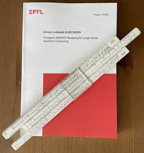
Cryogenic MOSFET Modeling for Large-Scale Quantum Computing
Arnout Lodewijk M BECKERS
Thèse n° 8365 2021
DOI: 10.5075/epfl-thesis-8365

Présentée le 28 mai 2021

Faculté des sciences et techniques de l’ingénieur Laboratoire de circuits intégrés Programme doctoral en génie électrique

pour l’obtention du grade de Docteur ès Sciences par
Arnout Lodewijk M BECKERS

Acceptée sur proposition du jury:
Prof. E. Charbon, président du jury
Prof. C. Enz, directeur de thèse
Prof. B. Parvais, rapporteur
Prof. G. Ghibaudo, rapporteur
Dr J.-M. Sallese, rapporteur 

Abstract: Promising results of state-of-the-art quantum computers fuel a world-wide effort in academic and private research laboratories to scale up the number of qubits and improve their characteristics in large arrays. To meet the scale-up challenge, innovative microelectronic architectures are envisioned hosting qubits and transistors in silicon. Integrated-circuit design for deep-cryogenic temperatures (below 10 K or -263.15°C) is a challenging optimization exercise that currently leads to costly iterations due to the lack of physics-based transistor models for these temperatures. Proposed enhancements to the industry-standard transistor models neglect the low-temperature physics and do not suffice for a large-volume application. This PhD thesis pushes the state-of-the-art of the characterization, physics, and modeling of CMOS (Complementary Metal Oxide Semiconductor) transistors down to deep-cryogenic temperatures. The most advanced commercial bulk CMOS technology (28-nm minimum gate length) is measured down to 4.2 K using dip-stick measurements and probe-station measurements. The temperature behavior of the physical parameters and the analog figures-of-merit is reported. A similar characterization study is presented for a 28-nm FDSOI CMOS technology using measurements provided by CEA-Léti through the EU H2020 MOS-Quito Project. It is shown that the design methodology based on the transconductance efficiency remains valid down to 4.2 K for both advanced CMOS processes. These results are already supporting the community: qubit controllers in 28-nm bulk and FDSOI technologies have been successfully deployed in the cryostats of quantum computers by Google and CEA-Léti, respectively. Industry-standard models have been honed over many years for near room-temperature operation. They show the largest discrepancies in the sub- and near-threshold regimes when used at deep-cryogenic temperatures. Therefore, this thesis presents an in-depth study of these regimes. Generalized Boltzmann relations are derived including band tails, which are valid in subthreshold. Using these relations, a new analytical theory is derived for the subthreshold swing that rolls off from the Boltzmann limit, showing that an ideal step-like switch cannot be obtained in the 0-K limit due to shallow band-edge states. The process quality must be improved to operate devices closer to the Boltzmann limit. Moreover, the transconductance efficiency in weak inversion (subthreshold) follows the new theoretical limit instead of the Boltzmann temperature limit. This mitigates the expected current savings from biasing in weak inversion. The new theory also explains the impossible inverse temperature dependence of the subthreshold-slope factor, which has been extracted in numerous characterizations in the literature. Furthermore, a threshold-voltage model for bulk CMOS is presented including dopant freezeout and interface traps. Process engineers can benefit from this model to customize transistors for use at 4.2 K. Finally, the discrepancy of the transfer characteristics in moderate inversion (near-threshold) is modeled with an improved representation of the localized band-edge states. As such, this PhD thesis lays the groundwork for next-generation deep-cryogenic IC design benefiting from physics-based knowledge. While this thesis is oriented toward quantum computing, the results also apply to other deep-cryogenic applications at the forefront of science and engineering.
Fig: Different explanations have been proposed for the deviation of the subthreshold swing (SS) from the Boltzmann limit at deep-cryogenic temperatures (below a critical temperature Tc). This led to the introduction of band-edge states to explain SS(T)