Fabia F. Athena, Xiangjin Wu, Nathaniel S. Safron, Amy Siobhan McKeown-Green, Mauro Dossena, Jack C. Evans, Jonathan Hartanto, Yukio Cho, Donglai Zhong, Tara Pena, Paweł Czaja, Parivash Moradifar, Paul C. McIntyre, Mathieu Luisier, Yi Cui, Jennifer A. Dionne, Greg Pitner, Iuliana P. Radu, Eric Pop, Alberto Salleo, H.-S. Philip Wong
Channel-last gate-all-around nanosheet oxide semiconductor transistor
arXiv:2512.21330v1 [cond-mat.mtrl-sci] 24 Dec 2025
1. Department of Electrical Engineering, Stanford University, Stanford (US)
2. Corporate Research, Taiwan Semiconductor Manufacturing Company, Ltd., San Jose (US)
3. Department of Chemistry, Stanford University, Stanford (US)
4. Department of Information Technology and Electrical Engineering, ETH Zurich (CH)
5. Department of Material Science and Engineering, Stanford University, Stanford (US)
6. Department of Chemical Engineering, Stanford University, Stanford (US)
7. Applied Energy Division, SLAC National Accelerator Laboratory, Menlo Park (US)
8. Institute of Metallurgy and Materials Science, Polish Academy of Sciences (PL)
9. Corporate Research, Taiwan Semiconductor Manufacturing Company, Ltd., Hsinchu (TW)
Abstract: As we move beyond the era of transistor miniaturization, back-end-of-line compatible transistors that can be stacked monolithically in the third dimension promise improved performance for low-power electronics. In advanced transistor architectures, such as gate-all-around nanosheets, the conventional channel-first process involves depositing dielectrics directly onto the channel. Atomic layer deposition of gate dielectrics on back-end-of-line compatible channel materials, such as amorphous oxide semiconductors, can induce defects or cause structural modifications that degrade electrical performance. While post-deposition annealing can partially repair this damage, it often degrades other device metrics. We report a novel channel-last concept that prevents such damage. Channel-last gate-all-around self-aligned transistors with amorphous oxide-semiconductor channels exhibit high on-state current (> 1mAμm) and low subthreshold swing (minimum of 63mV/dec) without the need for post-deposition processing. This approach offers a general, scalable pathway for transistors with atomic layer deposited channel materials, enabling the future of low-power three-dimensional electronics.

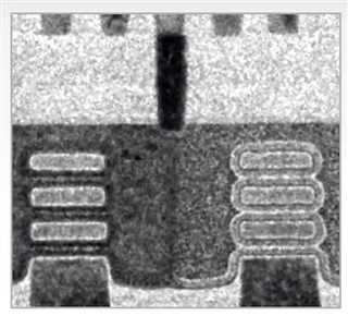
Fig: Electrical performance of CL GAA FETs. (A) A SEM image of a representative device structure and (B) an AFM image of IWO deposited on a control sample show a uniform and smooth surface. (C) IdVgs for a CL GAA FET with tch = 6nm measured at VDS = 0.05V and 1V. (D) IdVgs for a CL GAA FET with tch = 9 nm measured at VDS = 0.05V and 1V. Dual sweep shows very low hysteresis of about 0.038V at VDS = 0.05V.
Acknowledgment: Supported in part by SRC JUMP 2.0 PRISM and CHIMES Center, Stanford Differentiated Access Memory (DAM), SystemX Alliance, Stanford NMTRI, TSMC-Stanford Joint Development Project (P.C.M.). Part of this work was performed at Nano at Stanford (RRID SCR 026695). Authors acknowledge help and support for the AFM measurements from Christina Newcomb. Stanford authors thank MSS USA Corp. for high quality TEM sample preparation and examination and Dr. David Fried of Lam Research for providing access to Coventor SEMulator3D for process simulation. Use of the Stanford Synchrotron Radiation Lightsource at SLAC National Accelerator Laboratory is supported by the U.S. Department of Energy, Office of Science, Office of Basic Energy Sciences under Contract No. DE-AC02-76SF00515. Y.C. acknowledges the support from the Japan Society for the Promotion of Science (JSPS) overseas research fellowship. J.A.D., A.M.G., and P.M. acknowledge the financial support from the U.S. Department of Energy Office of Science National Quantum Information Science Research Centers as part of the Q-NEXT center. Y.C. and F.F.A. would like to thank the support from the Stanford Energy Postdoctoral Fellowship and Precourt Institute for Energy.