Matteo Farronato, Fabio Carletti, Niccolò Garegnani, Anupam Jana, Matteo Porzani, Saverio Ricci, Augusta Ungarelli, Christian Monzio Compagnoni, Paolo Fantini, Innocenzo Tortorelli, Agostino Pirovano, Christian Rinaldi and Daniele Ielmini
Voltage-controlled reconfigurable characteristics in MoS2 transistors
via ion migration for reprogrammable logic.
NPJ 2D Mater Appl (2026)
DOI: 10.1038/s41699-026-00720-2
1 DEIB, Politecnico di Milano and IU.NET, Milano, Italy
2 Dipartimento di Fisica, Politecnico di Milano, Italy
3 Micron Technology Inc., Vimercate (MB), Italy
Abstract: 2D semiconductors such as MoS2 offer a promising pathway for future logic and analog transistors and memories. These materials feature scalable channel size, back-end of the line compatibility, and high mobility for relatively small channel thickness approaching few atomic monolayers. An open issue for the development of mature 2D-based digital technology is the availability of both n- and p-type transistors, as well as the ability to control the transistor type in a reconfigurable way. This work presents a novel MoS2-based transistor exhibiting reconfigurable n- or p-type characteristics, namely switching from n-type to p-type and vice versa, which is attributed to ion-assisted doping from the gate dielectric layer. Extensive characterization of the device shows repeatable switching with relatively low cycle-to-cycle (C2C) and device-to-device (D2D) variability. A reconfigurable p-n junction is demonstrated via a junction-less multi-gate MoS2-based transistor. We also demonstrate various reconfigurable logic gates, including a complementary metal-oxide-semiconductor (CMOS) inverter, a fully n-type inverter and an XNOR logic gate based on MoS2 transistors, showcasing the generality and flexibility of channel reconfiguration for logic circuit applications. These results underscore the strong potential of reconfigurable MoS2 transistors for ultra-scaled, reconfigurable logic circuits.

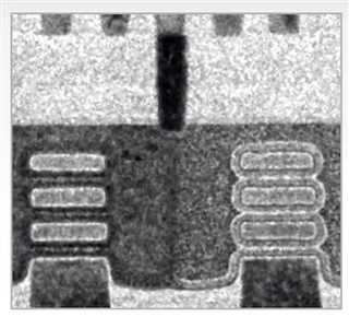
Fig: Logic gates with reconfigurable MoS2 transistors. (a) SEM image of a logic inverter or CMOSNOT gate with two transistors in the same MoS2 flake. (b) Schematic of the inverter with reconfigurable MoS2 transistors and logic truth table.
Acknowledgments: This article has received funding from the European Research Council (ERC) under the EuropeanUnion’s Horizon Europe Research and Innovation Programme (grant 101054098). Authors want tothank all the Polifab (the micro and nano technology infrastructure of Politecnico di Milano) staff fortheir help in the fabrication of the MoS2-based devices.