Jan 7, 2025
[paper] MOSFET-Based Voltage Reference Circuits
Feb 19, 2021
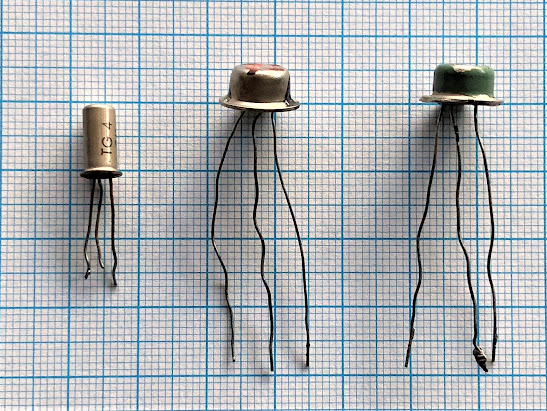
Virtual Si Museum /2107/ TG4 and TG50
The TG1-TG5 series transistor are the first industrially mass-produced BJT transistors in Poland. The serial production was started by the TEWA Semiconductor Factory, Warsaw, in early1960s. Then, the TG50-TG55 series, was also manufactured by the TEWA in 1961–1962.
The TG4 (see Pic: below) is low power, low frequency, pnp germanium (Ge) alloy transistor (with 75 mW max collector power) [1].
The TG50 (below) is medium power, low frequency, pnp germanium (Ge) alloy transistor (with 175 mW max collector power) [2].
An initial stage of Polish semiconductor microelectronics research activities has been reviewed by Prof. Jerzy Pułtorak. In his paper [3], he has reviewed activities of leading Polish R&D groups starting from Department of Electronics, Polish Academy of Sciences (PAN) founded on July 4, 1952 till foundation of the Instytut Technologii Elektronowej (ITE, Warsaw) early 1960 (now Sieć Badawcza Łukasiewicz - Instytut Mikroelektroniki i Fotoniki). The first, in Poland, experimental germanium point-contact transistor TP-1 [4] has been developed by Prof. Rosinski just after John Bardeen, Walter Brattain and William Shockley have invented a semi-conductor triode (transistor) [5] on December 23, 1947.
Jan 6, 2021
Virtual Si Museum /2101/ Electron Devices Time Line
my own view on the electron devices time line. The electron devices scaling: from a single vacuum tube, a BJT, TTL digital ICs to 68719476736 devices in a NAND flash memory card. If you have something else to add, just let me know:
REF:- Vacuum Tube GE 9-22 188-5
- 2N2905A BJT - PNP, -60 V, -600 mA, 600 mW, TO-39
- TTL 74F00 IC - 5V, quad 2-input NAND gate; series F (=fast) introduced in 1978
- 64Gb NAND flash memory card
Apr 24, 2020
Online Classes on The Principle of Semiconductor Devices
- Principle of Semiconductor Devices Part I: Semiconductors, PN Junctions and Bipolar Junction Transistors
An intuitive approach to operational principles of semiconductor devices.The course covers PN junction diodes, optical sensors, solar cells, LEDs, and Bipolar Junction Transistors.
https://www.edx.org/course/principle-of-semiconductor-devices-part-i-semiconductors-pn-junctions-and-bipolar-junction-transistors-1 - Principle of Semiconductor Devices Part II: Field Effect Transistors and MOSFETsAn intuitive approach to operational principles of semiconductor devices. The course covers MOS capacitors, charge coupled devices, classical MOSFETs, transistor scaling, short channel MOSFET, and nano-CMOS transistors.
https://www.edx.org/course/principle-of-semiconductor-devices-part-ii-field-effect-transistors-and-mosfets-2
Meet your instructor:

Mar 23, 2020
MicroTec: Semiconductor Process and Device Simulator
Jun 15, 2016
[book] Compact Models for Integrated Circuit Design
- Presents industry standard models for bipolar-junction transistors (BJTs), metal-oxide-semiconductor (MOS) field-effect-transistors (FETs), FinFETs, and tunnel field-effect transistors (TFETs), along with statistical MOS models
- Discusses the major issue of process variability, which severely impacts device and circuit performance in advanced technologies and requires statistical compact models
- Promotes further research of the evolution and development of compact models for VLSI circuit design and analysis
- Supplies fundamental and practical knowledge necessary for efficient integrated circuit (IC) design using nanoscale devices
- Includes exercise problems at the end of each chapter and extensive references at the end of the book
Sep 1, 2015
[video] How to Model a BJT Bipolar Junction Transistor
Video Published on Aug 31, 2015
To download the project files referred to in this video visit:
http://www.keysight.com/find/eesof-how-to-model-BJT
Apr 3, 2014
VI Regional Seminar MNE & MS 2014
- С.И. Матюхин1, Welcome and Seminar Openning,
1Госуниверситет-УНПК - Турин В.О.1, Кильчицкая М.В.2, Герасимов К.А.2, Simulation of power bipolar transistor,
1Госуниверситет-УНПК, 2БГТУ, г. Брянск - Ващенко В.А., The physical ESD design for integrated circuits and electronic devices,
Maxim Integrated Corp., г. Сан Хосе, Калифорния, США - Цырлов А.М., Development of CMOS optocoupler,
ОАО «Протон», г. Орёл - Студенников А.С., Development of CMOS ICs,
ОАО «Протон», г. Орёл - Малый Д.О.1, Матюхин С.И.2, Ставцев А.В.1, "Proton-Elektroteks" IGBT-devices JSC: basic approaches of production and quality assurance,
1ЗАО «Протон-Электротекс», г. Орёл, 2Госуниверситет-УНПК - Макулевский Г.Р., Матюхин С.И., Current-voltage characteristics of laser diodes based on AlGaAs,
Госуниверситет-УНПК - Матюхин С.И., Гришин В.О., Radiation effects of on the current-voltage characteristic of power diodes and thyristors,
Госуниверситет-УНПК - Писарев А.А.1, Матюхин С.И.2, Сурма А.М.1, Черников А.А.1, Electrical characteristics of fast diodes with soft recovery,
1ЗАО «Протон-Электротекс», г. Орёл, 2Госуниверситет-УНПК - Koziol Z., Aestimo quantum mechanical software for modeling quantum wells in nanoelectronics,
TU Rzeszow, Polska
May 1, 2013
13th HICUM Workshop 2013
Workshop Highlights:
- Special presentation by Prof. Spirito on mm-wave on-wafer measurements
- Various presentations covering the modeling of various bipolar transistor phenomena, new parameter extraction strategies, production-type model development, model testing and performance comparisons
- Special presentations on benchmark circuits for model verification (solicited)


