Core partners
Dec 8, 2021
Discover DIH-Network and their services
Dec 7, 2021
[mos-ak] [Final Program] 14th International MOS-AK Workshop Silicon Valley, Dec. 17, 2021
Registered participants will receive online meeting invitation 24h before the event.(any related enquiries can be sent to register@mos-ak.org)
- Call for Papers: Oct. 2021
- 2nd Announcement: Nov. 2021
- Final Workshop Program: Dec.2 2021
- MOS-AK Workshop: Dec.17, 2021
in timeframe of IEDM and Q4 CMC Meetings
(Silicon Valley Time Zone / GMT-8)
10:00am - 12:30pm MOS-AK Morning Session
1:00pm - 3:30pm MOS-AK Afternoon Session
You received this message because you are subscribed to the Google Groups "mos-ak" group.
To unsubscribe from this group and stop receiving emails from it, send an email to mos-ak+unsubscribe@googlegroups.com.
To view this discussion on the web visit https://groups.google.com/d/msgid/mos-ak/CALp-Rj9VuWP7MtEJPWSQJhW9x3B1KAnb%3Di2gO6EFpU%3DsXcfCJg%40mail.gmail.com.
Dec 3, 2021
#RISC-V grows #opensource #processor membership 130% in 2021 https://t.co/jK3BHOYbrL #semi https://t.co/WNUecB8IH6
— Wladek Grabinski (@wladek60) Dec 3, 2021
from Twitter https://twitter.com/wladek60
December 03, 2021 at 09:47AM
via IFTTT
Dec 1, 2021
#Efabless Corporation shuttle at #SkyWater #Technology #Foundry sponsored by #Google #FOSS #FOSSi #semi #chips #opensource #PDK #MPW https://t.co/qFDu2gyJki
— Wladek Grabinski (@wladek60) Dec 1, 2021
from Twitter https://twitter.com/wladek60
December 01, 2021 at 10:47AM
via IFTTT
Nov 30, 2021
[Open Hardware] [CfP] Computer Aided Modeling and Design Development Room
We hope you'll join us for a full day of talks, demos and interesting
discussions on designing, modeling and testing physical objects using
Open Source tools. This year's event will be fully virtual (:sad trombone:)
and will feature multiple channels for talks, Q&A as well as
hallway discussions (:happy dance:).
We welcome any talk proposals about the creation of physical objects.
Topics of interest include, but are not limited to:
* Printed circuit board design tools
* Circuit simulation
- 3d modeling and analysis
* Solid modeling tools
* Meshing, modeling and transforming physical representations
* Finite element analysis
- 3d printing
* 3d slicing tools
* Motor control
- Machine design and integration
* ECAD/MCAD integration
* Thermal analysis
* Wire modeling
- Physical Model Data storage
* Data representation and optimization
* Version control in hardware data storage
* Collaborative and team-based hardware design techniques
Slots will be allocated for short (20 minutes), long (40 minutes)
talks and in-depth (60 minutes). This includes question time, for which
questions and answers.
Depending on the number of submissions, submitters may be asked to
utilize an alternate time format.
## The submission process
Please submit your proposals at
https://penta.fosdem.org/submission/FOSDEM22
If you already have a Pentabarf account (for example as a result of
having submitted a proposal in the past), make sure you use it to log in
and submit your proposal. Do not create a new account if you already
have one.
Please include the following information with your submission:
- Abstract
- Preferred Session length
- Speaker bio
- Link to any hardware / code /slides for the talk
When you submit your proposal (creating an "Event" in Pentabarf), make
sure you choose the "Open Source Computer Aided Modeling and Design" in
the track drop-down menu. Otherwise your proposal may go unnoticed.
Fill in at least a title and abstract for the proposed talk and a
suggested duration. Keep in mind that much of the value in these
meetings comes from the discussions, so please allot at least 20%
## Important dates
- Call for papers available: 29 November 2021
- Call for participation closes: 28 December 2021
- Devroom schedule available: 1 January 2022
## Recordings
content (CC-BY).
open-hardware-devroom mailing list
open-hardware-devroom@lists.fosdem.org
https://lists.fosdem.org/listinfo/open-hardware-devroom
Nov 27, 2021
[paper] Bridging the gap between design and simulation of low voltage CMOS circuits
Nov 24, 2021
ESSCIRC/ESSDERC 2021 The Best Paper Awards
- BEST JOINT PAPER 2021: “Low Power Indirect Time-of-Flight Pixel Achieving 88.5% Demodulation Contrast at 200MHz for 0.54MPix Depth Camera” by Cedric Tubert et al., STM (F)
- BEST STUDENT JOINT PAPER 2021: “Cryogenic Characterization and Modeling of 14 nm Bulk FinFET Technology”, by @Asma Chabane, IBM Research GmbH
- BEST ESSDERC PAPER 2021: “Complementary Two-Dimensional (2-D) MoS_2 FET Technology”, by @Cristine Jin Estrada et al., The Hong Kong UST
- BEST ESSDERC STUDENT PAPER 2021:“VERILOR: a Verilog-a Model of Lorentzian Spectra for Simulating Trap-Related Noise in CMOS Circuits”, by @Angeliki Tataridou, IMEP-LaHC, UniversitĆ© Grenoble Alpes, University Savoie Mont Blanc, CNRS, Grenoble INP
- BEST ESSCIRC PAPER 2021: “A Resolution-Adaptive 8mm2 9.98Gb/S 39.7pJ/B 32-Antenna All-Digital Spatial Equalizer for mmWave Massive MU-MIMO in 65nm CMOS”, by @Oscar Castaneda et al., ETH Zürich and Cornell Univ.
- BEST ESSCIRC STUDENT PAPER 2021:”A −109.1 dB/−98 dB THD/THD+N Chopper Class-D Amplifier with >83.7 dB PSRR Over the Entire Audio Band”, by @Huajun Zhang et al., TU Delft
Nov 23, 2021
MPW-4 is open! Deadline is December 31, 2021
[https://t.co/H9QtSVW2z9] MPW-4 is open! Deadline is December 31, 2021. #Free fabrication for #opensource #chip projects. #semi #manufacturing #pdk #IC #SPICE https://t.co/zVCswKFbcL
— Wladek Grabinski (@wladek60) Nov 23, 2021
from Twitter https://twitter.com/wladek60
November 23, 2021 at 05:25PM
via IFTTT
Samsung, 2nm will go into mass production in the 2nd Half of 2025
According to Samsung, 2nm will go into mass production in the 2nd Half of 2025 using a 3rd generation Gate-All-Around Field Effect Transistor Architecture (#GAA #FET) [https://t.co/gKjXIv5IPM] #GAAFET #Samsung #Foundry #semi #chips https://t.co/a8sUsp5KLm

— Wladek Grabinski (@wladek60) Nov 23, 2021
from Twitter https://twitter.com/wladek60
November 23, 2021 at 05:28PM
via IFTTT
Nov 22, 2021
[paper] ACM Model for CMOS Analog Circuits Hand Design
a Instituto Federal da Bahia, Santo Amaro, Brazil
b DEEC, Escola PolitƩcnica, Universidade Federal da Bahia, Salvador, Brazil
Nanorennes (CNRS)
Nov 19, 2021
[paper] TFT XNOR/XOR Circuit
Acknowledgement: Devices were fabricated on the NanoRennes platform.
My Story of Raja Manickam, CEO of OSAT, Tata Electronics
Nov 17, 2021
[mos-ak] 2nd Announcement and C4P] 14th International MOS-AK Workshop Silicon Valley, Dec. 17, 2021
- Compact Modeling (CM) of the electron devices
- Advances in semiconductor technologies and processing
- Verilog-A language for CM standardization
- New CM techniques and extraction software
- Open Source (FOSS) TCAD/EDA modeling and simulation
- CM of passive, active, sensors and actuators
- Emerging Devices, Organic TFT, CMOS and SOI-based memory
- Microwave, RF device modeling, high voltage device modeling
- Nanoscale CMOS, BiCMOS, SiGe, GaN, InP devices and circuits
- Technology R&D, DFY, DFT and reliability/aging IC designs
- Foundry/Fabless Interface Strategies
- Call for Papers: Oct. 2021
- 2nd Announcement: Nov. 2021
- Final Workshop Program: Dec.2 2021
- MOS-AK Workshop: Dec.17, 2021
in timeframe of IEDM and Q4 CMC Meetings
You received this message because you are subscribed to the Google Groups "mos-ak" group.
To unsubscribe from this group and stop receiving emails from it, send an email to mos-ak+unsubscribe@googlegroups.com.
To view this discussion on the web visit https://groups.google.com/d/msgid/mos-ak/CALp-Rj_9dbmiZsqt0CUx8AcsAy1ct4HjagqJw374%2BEa_zLfEyA%40mail.gmail.com.
[https://t.co/phyxhOdhdm] Duisburg RISC-V 4th International Meetup https://t.co/YdSvOTXMUG #serv #riscv #fossi #fusesoc #semi #chips https://t.co/nnZywb4LEk
[https://t.co/phyxhOdhdm] Duisburg RISC-V 4th International Meetup https://t.co/YdSvOTXMUG #serv #riscv #fossi #fusesoc #semi #chips https://t.co/nnZywb4LEk
— Wladek Grabinski (@wladek60) Nov 17, 2021
from Twitter https://twitter.com/wladek60
November 17, 2021 at 10:43AM
via IFTTT
[https://t.co/sIRWwTkifR] The #Chip That Could #Transform #Computing #semi #semiconductors #manufacturing https://t.co/SxOqFf712o
[https://t.co/sIRWwTkifR] The #Chip That Could #Transform #Computing #semi #semiconductors #manufacturing https://t.co/SxOqFf712o
— Wladek Grabinski (@wladek60) Nov 17, 2021
from Twitter https://twitter.com/wladek60
November 17, 2021 at 10:34AM
via IFTTT
The Semiconductor Manufacturing Road Map For India (by Chetan Arvind Patil ) #semiconductorindustry #semi #technology #manufacturing #ic #icdesign #foundry #foundries #idm #chips https://t.co/dxkDdFbqd4
— Wladek Grabinski (@wladek60) Nov 17, 2021
from Twitter https://twitter.com/wladek60
November 17, 2021 at 10:09AM
via IFTTT
Nov 16, 2021
[paper] Extended gate FET pH Sensor
College of Engineering, UiTM, Selangor (MY)
[C4P] FLEPS 2022
Topics of Interest
- Organic/Inorganic Electronic Sensors
- Emerging Materials for Flexible and Printable Systems
- Manufacturing Techniques
- High-throughput Printable Electronics
- Hybrid Flexible Sensors and Electronics
- Stretchable/Shrinkable Sensors and Electronics
- Soft/Smart Wearable and Implantable Sensing Systems
- Disposable/Reusable Sensors and Electronics
- Printed Large-Area Sensors and Systems
- Flexible or Printed Active and Passive Components (e.g. actuators, printed energy devices, smart labels, RFID etc.)
- Emerging applications of Flexible Electronics inc. IoT, smart cities etc.
- Simulation and Modelling
- Flexible/Printable Electronics in context with Circular Economy and green electronics
For further information, contact Coral Miller at Conference Catalysts, LLC.
Nov 15, 2021
[paper] Nanoscale InGaAs FinFETs
1: Microsystems Technology Laboratories, MIT, Cambridge (USA)
2: Analog Devices, Inc., (USA)
3: IPT Center, Universidad PolitƩcnica de Madrid (SP)
The panel: #UK Should Emulate #Israel for #Semiconductor #Startups to Succeed
The panel: Where are we now, where do we want to go? #UK Should Emulate #Israel for #Semiconductor #Startups to Succeed - EE Times Europe https://t.co/LpfK6H2mnU #semi #chips https://t.co/SPuqTG2p4W
— Wladek Grabinski (@wladek60) Nov 15, 2021
from Twitter https://twitter.com/wladek60
November 15, 2021 at 01:49PM
via IFTTT
[book] Future Ultra Low Power Electronics
Abstract: This book covers the fundamentals and significance of 2-D materials and related semiconductor transistor technologies for the next-generation ultra low power applications. It provides comprehensive coverage on advanced low power transistors such as NCFETs, FinFETs, TFETs, and flexible transistors for future ultra low power applications owing to their better subthreshold swing and scalability. In addition, the text examines the use of field-effect transistors for biosensing applications and covers design considerations and compact modeling of advanced low power transistors such as NCFETs, FinFETs, and TFETs. TCAD simulation examples are also provided.
Contents:Preface viiEditors ixContributors xi
Chapter 1: An Introduction to Nanoscale CMOS Technology Transistors: A Future Perspective; pp: 1
Kumar Prasannajit Pradhan
Chapter 2: High-Performance Tunnel Field-Effect Transistors (TFETs) for Future Low Power Applications; pp: 29
Ribu Mathew, Ankur Beohar, and Abhishek Kumar Upadhyay
Chapter 3: Ultra Low Power III-V Tunnel Field-Effect Transistors; pp: 59
J. Ajayan and D. Nirmal
Chapter 4: Performance Analysis of Carbon Nanotube and Graphene Tunnel Field-Effect Transistors; pp: 87
K. Ramkumar, Singh Rohitkumar Shailendra, and V. N. Ramakrishnan
Chapter 5: Characterization of Silicon FinFETs under Nanoscale Dimensions; pp: 115
Rock-Hyun Baek and Jun-Sik Yoon
Chapter 6: Germanium or SiGe FinFETs for Enhanced Performance in Low Power Applications; pp: 129
Nilesh Kumar Jaiswal and V. N. Ramakrishnan
Chapter 7: Switching Performance Analysis of III-V FinFETs .; pp: 155
Arighna Basak, Arpan Deyasi, Kalyan Biswas, and Angsuman Sarkar
Chapter 8: Negative Capacitance Field-Effect Transistors to Address the Fundamental Limitations in Technology Scaling; pp: 187
Harsupreet Kaur
Chapter 9: Recent Trends in Compact Modeling of Negative Capacitance Field-Effect Transistors; pp: 203
Shubham Tayal, Shiromani Balmukund Rahi, Jay Prakash Srivastava, and Sandip Bhattacharya
Chapter 10 Fundamentals of 2-D Materials; pp: 227
Ganesan Anushya, Rasu Ramachandran, Raj Sarika, and Michael Benjamin
Chapter 11 Two-Dimensional Transition Metal Dichalcogenide (TMD) Materials in Field-Effect Transistor (FET) Devices for Low Power Applications; pp 253
R. Sridevi and J. Charles Pravin
Index pp: 289
[paper] Verilog-A Compact MTJ Model
Nov 13, 2021
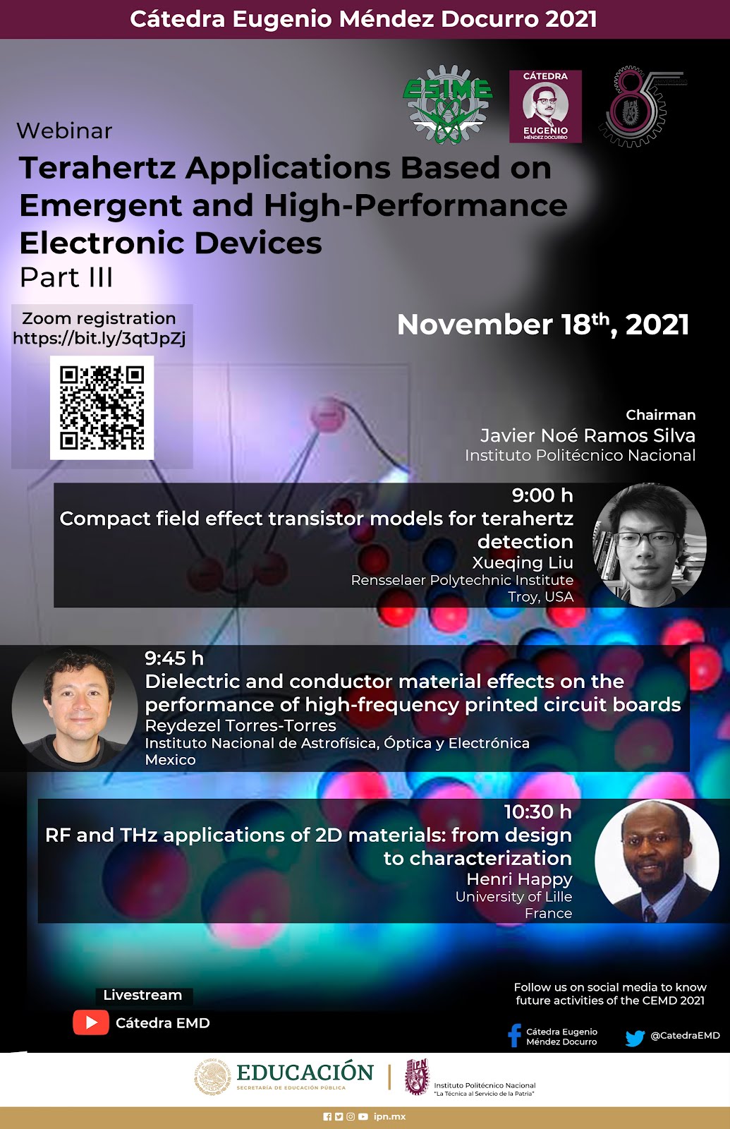
Advances in RF and THz emerging electronic devices webinar at IPN-UAB
- AnĆbal Uriel Pacheco Sanchez or
- Eloy Ramirez Garcia, IPN co-organizer
Nov 11, 2021
Career opportunities at VTT
VTT is one of the leading research organizations in Europe and we are operating the largest R&D cleanroom in the Nordic countries, located in Micronova premises, Espoo. We develop innovative micro, nano and quantum systems and algorithms and software driven by different sensing, communication and computing applications. A timely example being the building of Finland's first quantum computer. We work closely with global industrial and academic players of different fields of technology. What unites us at VTT are the curiosity, passion of learning and devotion to finding solutions to global challenges and answers to our customers' needs. You can familiarize with us further by exploring VTT's research infra through VTT World.
Due to our continual growth, we are currently seeking for more than 15 new talents in microelectronics and quantum technologies to join our team. If you are interested in joining VTT, read more about job opportunities using links below:
- Summary of all job openings in Microelectronics and Quantum Technologies teams
- Research Scientist, Superconducting Quantum Circuits
- Research Scientist, Quantum Hardware Development
- Senior / Research Scientist, Digital Electronics and Embedded Software
- Research Scientist, Quantum Algorithms and Software
- Research Scientist, Neuromorphic Computing Algorithms and Software
- Research Scientist, Nanoelectronic Devices
- Research Scientist, Photonic and Thermal Devices
- Two Senior / Research Scientists, Analog IC Design for Neuromorphic Computing
- Research Scientist, Silicon Photonics Process Integration
- Research Scientist, Optical Computing and Quantum Photonics Hardware
- Research Technicians, Cleanroom
- Mechanical Designer
- Master's Thesis Worker, Low Temperature Physics
- Master's Thesis Worker, Photonic and Thermal Devices
- Master's Thesis Worker, Nanoelectronic Devices
- Master's Thesis Worker, Graphene Quality Control
Best regards
Matteo Cherchi, PhD
Senior Scientist
Tel. +358 40 6849040
- - - - - - - - - - - - - -
VTT
Micronova
Tietotie 3, Espoo, Finland
Find us in social media:
Facebook Instagram LinkedIn Twitter Youtube
The information in this e-mail and any attachment is confidential. If you have received it in error, any use of the e-mail by you is prohibited. Please notify the sender immediately and delete the original.
[paper] InP HEMTs for future THz applications
a SR University, Warangal, Telangana, India
b Karunya Institute of Technology and Sciences, Coimbatore, Tamilnadu, India
c VIT Bhopal University, Bhopal, Madhya Pradesh, India
d Kerala Technological University, Trivandrum, Kerala, India
e Sona College of Technology, Salem, Tamilnadu, India
f Sreenidhi Institute of Science and Technology, Hyderabad, Telangana, India