Sep 14, 2020

[mos-ak] Fwd: ESSCIRC ESSDERC 2020 Virtual Educational Events | IMPORTANT MESSAGE

ESSCIRC ESSDERC 2020 VIRTUAL EDUCATIONALS
LIVE EXECUTIVE SESSIONS: September 14, 15 
ON DEMAND September 7 - October 16

Hello,
You are receiving this message because you registered for the ESSCIRC ESSDERC 2020 Virtual Educational Events.

How is it going so far? 
Feel free to use the Q&A box to send us questions: all questions will be gathered end of the week and will be transmitted to the event organizers prior to the Live events next week.

Take also advantage of the POLLS in the following Educational Events: 

3. WORKSHOP | Non-Volatile Memories: Opportunities and Challenges from Devices to Systems
10. DISSEMINATION WORKSHOP |  Toward sustainable IOT from rare materials to big data
11. DISSEMINATION WORKSHOP | High Density 3D CMOS Mixed-Signal Opportunities
12. MOS-AK WORKSHOP | Compact/SPICE Modeling and its Verilog-A Standardization

Questions and polls will be discussed during the LIVE EXECUTIVE SESSIONS.
How to access the Live Executive Sessions?
Once logged in, you see a small window on the left called "ADDITIONAL RESOURCES": the hyperlink to live session is there and, of course, it will be active only during live sessions 

Last but not least, if you are experiencing some connections problems while using your office PC, check with your IT staff if firewalls prevent you from connecting to the on-line virtual events. 

See you there!
ORGANIZING COMMITTEE
Thomas Ernst (CEA-LETI, FR), General co-chair
Dominique Thomas (STMicroelectronics, FR), General co-chair

François Andrieu (CEA-LETI, FR), ESSDERC TPC Chair
Maud Vinet (CEA-LETI, FR), ESSDERC TPC co-Chair

Andreia Cathelin (STMicrolectronics, FR), ESSCIRC TPC Chair
Sylvain Clerc (STMicrolectronics, FR), ESSCIRC TPC co-Chair

2020 Virtual Educationals Chairs
Sylvain Clerc (STMicrolectronics, FR)
Ionut Radu (SOITEC, FR)

LOCAL EXECUTIVE SECRETARIAT
Sandra Barbier (CEA-LETI, FR) | sandra.barbier@cea.fr

ORGANIZING SECRETARIAT
Sistema Congressi s.r.l. | essxxrc@sistemacongressi.com 

JOIN NOW OUR 
ESSCIRC – ESSDERC
LinkedIn group!

Share Share
Forward Forward
ORGANIZERS
TECHNICAL SPONSORSHIP

FINANCIAL SPONSORSHIP
DIAMOND SPONSOR

WATCH ME
Copyright © 2020 Sistema Congressi s.r.l., All rights reserved.
You are receiving this email because you registered for ESSCIRC ESSDERC 2020 Virtual Events

Our mailing address is:
Sistema Congressi s.r.l.
Via Trieste 26
Padova, PD 35121
Italy

Add us to your address book


--
You received this message because you are subscribed to the Google Groups "mos-ak" group.
To unsubscribe from this group and stop receiving emails from it, send an email to mos-ak+unsubscribe@googlegroups.com.
To view this discussion on the web visit https://groups.google.com/d/msgid/mos-ak/CALp-Rj_4EzeNd1cNwE-Jfx8nsGBrcSH3vN3KTxttAX2enMx96g%40mail.gmail.com.

2020 IEEE #IEDM To Highlight Innovative Devices for a #Better #Future


from Twitter https://twitter.com/wladek60

September 14, 2020 at 10:25AM
via IFTTT

Sep 9, 2020

[paper] Analogue 2D Semiconductor Electronics

Analogue two-dimensional semiconductor electronics
Dmitry K. Polyushkin1, Stefan Wachter1, Lukas Mennel1, Matthias Paur1, Maksym Paliy2, Giuseppe Iannaccone2, Gianluca Fiori2, Daniel Neumaier3,4, Barbara Canto3,4
and Thomas Mueller1
Nat Electron 3, 486–491 (2020)
DOI: 10.1038/s41928-020-0460-6

1Vienna University of Technology, Institute of Photonics, Vienna, Austria. 
2Dipartimento di Ingegneria dell’Informazione, Università di Pisa, Pisa, Italy.
3AMO GmbH, Aachen, Germany. 
4Bergische Universität Wuppertal, Wuppertal, Germany

Abstract: Digital electronics are ubiquitous in the modern world, but analogue electronics also play a crucial role in many devices and applications. Analogue circuits are typically manufactured using silicon as the active material. However, the desire for improved performance, new devices and flexible integration has—as for their digital counterparts—led to research into alternative materials, including the use of two-dimensional (2D) materials. Here, we show that operational amplifiers—a basic building block of analogue electronics—can be created using the 2D semiconductor molybdenum disulfide (MoS2) as the active material. The device is capable of stable operation with good performance, and we demonstrate its use in feedback circuits including inverting amplifiers, integrators, log amplifiers and transimpedance amplifiers. We also show that our 2D platform can be used to monolithically integrate an analogue signal preconditioning circuit with a MoS2 photodetector.

Fig: a) Schematic of the back-gated transistor architecture; 
b) Transfer characteristics of a typical transistor on the chip (W/L = 4); 
c) View of a single OPA showing the pinout and transistor labelling

Circuit design and modelling: Because a complete model of back-gated 2D semiconductor FETs is still not readily available, we fitted the experimental results with an Enz–Krummenacher– Vittoz (EKV) model in both, the subthreshold and inversion, regimes. All the transistors operate in the inversion regime, we used the inversion model to simulate the OPA, obtaining a nominal low-frequency Atot gain value.

Acknowledgements: We thank A.J. Molina-Mendoza for technical assistance and N. Schaefer and J.A. Garrido for providing a polyimide substrate. We acknowledge financial support by the European Union (grant agreements 785219 Graphene Flagship, 796388 ECOMAT and 828901 ORIGENAL), the Austrian Science Fund FWF (START Y 539-N16) and the Italian MIUR (FIVE 2D).

Electronic Frontier Foundation Turns 30 This Year! Learn More About #EFF, and How You Can Help. https://t.co/jDPakWReaO #OpenSource https://t.co/7bDPyRYenl


from Twitter https://twitter.com/wladek60

September 09, 2020 at 09:15AM
via IFTTT

Sep 8, 2020

#India now ranks among the #Top10 countries in terms of the number of #opensource projects [https://t.co/5VnCn8CErA] https://t.co/v2IsUB9ZZL https://t.co/ScATobwByx


from Twitter https://twitter.com/wladek60

September 08, 2020 at 03:27PM
via IFTTT

[paper] RF Small-Signal Model for Four-Port Network MOSFETs

A High-Frequency Small-Signal Model for Four-Port Network MOSFETs
Alejandro Roman-Loera1, Member, IEEE, Anurag Veerabathini2, Member, IEEE, Luis A.Flores-Oropeza1, Member, IEEE, and Jaime Ramirez-Angulo3, Life Fellow, IEEE
IEEE 63rd IMWSCAS 2020
DOI:10.1109/mwscas48704.2020.9184475 

1Electronic Systems Department, Universidad Autonoma de Aguascalientes, Mexico.
2Maxim Integrated, Chandler, AZ, USA.
3Klipsch School of Electrical and Computer Engineering, New Mexico State University, Las Cruces, NM, USA.

Abstract: A high-frequency small-signal model for a MOSFET is proposed considering the parasitic capacitances associated with each terminal that is critical in the design of high-frequency amplifiers. The proposed model allows in obtaining a closed form expression for poles and zeros due to parasitic elements along with the conventional poles and zeros. This model gives an additional degree of freedom in choosing the location of poles and zeros to improve the frequency response. The proposed high-frequency small-signal model for MOSFET is validated in simulation by implementing a high-frequency voltage follower in 0.18µm CMOS process. The proposed model shows the existence of a zero in a voltage follower that is introduced by the parasitic elements at high-frequencies and it is validated with implementation.

Fig: Small signal equivalent circuit of a 4-port MOSFET (a) Conventional model, (b) Model with substrate parasitics, and (c) Model with additional parasitics, and (d) Proposed model.

Acknowledgment: This work has been supported by PRODEP program from SEP (Secretariat of Public Education, Mexico) and Universidad Autonoma de Aguascalientes, Aguascalientes, Mexico.

Sep 7, 2020

#25 #Microchips That Shook the #World - IEEE Spectrum https://t.co/XCdh3S0ClW #semi https://t.co/JFWuLICVDT

1968 Fairchild Semiconductor μA741 Op-Amp
1971 Signetics NE555 Timer
1971 Western Digital WD1402A UART
1973 Mostek MK4096 4-Kilobit DRAM
1975 MOS Technology 6502 Microprocessor
1976 Zilog Z80 Microprocessor
1978 Texas Instruments TMC0281 Speech Synthesizer
1979 Intel 8088 Microprocessor
1979 Motorola MC68000 Microprocessor
1983 Intersil ICL8038 Waveform Generator
1983 Texas Instruments TMS32010 Digital Signal Processor
1985 Acorn Computers ARM1 Processor
1985 Chips & Technologies AT Chip Set
1985 Xilinx XC2064 FPGA
1986 Kodak KAF-1300 Image Sensor
1987 Sun Microsystems SPARC Processor
1987 Texas Instruments Digital Micromirror Device
1988 Computer Cowboys Sh-Boom Processor
1989 Toshiba NAND Flash Memory
1993 Microchip Technology PIC 16C84 Microcontroller
1994 Amati Communications Overture ADSL Chip Set
1997 IBM Deep Blue 2 Chess Chip
1997 Micronas Semiconductor MAS3507 MP3 Decoder
1998 Tripath Technology TA2020 AudioAmplifier
2000 Transmeta Corp. Crusoe

from Twitter https://twitter.com/wladek60

September 07, 2020 at 03:57PM
via IFTTT

[paper] Vertical Graphene–hBCN Heterostructure TFETs

A comparative computational study of tunneling transistors
based on vertical graphene–hBCN heterostructures
Mahsa Ebrahimi1, Ashkan Horri1, Majid Sanaeepur2, and Mohammad Bagher Tavakoli1
J. Appl. Phys. 127, 084504 (2020); DOI: 10.1063/1.5130777
Published Online: 28 February 2020

1Department of Electrical Engineering, Arak Branch, Islamic Azad University, Arak, Iran
2Department of Electrical Engineering, Faculty of Engineering, Arak, Iran

ABSTRACT In this paper, the electrical characteristics of tunneling transistors based on vertical graphene and a hexagonal boron-carbon-nitrogen (hBCN) heterostructure are studied and compared theoretically. We have considered three different types of hBCN, i.e., BC2N, BC2N0, and BC6N as a tunneling barrier. Our simulation is based on the nonequilibrium Green’s function formalism along with an atomistic tightbinding (TB) model. The TB parameters are obtained by fitting the band structure to first-principles results. By using this method, electrical characteristics of the device, such as the ION=IOFF ratio, subthreshold swing, and intrinsic gate-delay time, are investigated. For a fair comparison, the effects of geometrical variations and number of tunneling barrier layers on the electrical parameters of the device are simulated and investigated. We show that, by an appropriate design, the device can be used for low-power or high-performance applications. The device allows current modulation exceeding 106 at room temperature for a 0.6 V bias voltage.

FIG. DFT Band structure for (a) graphene - hBC2N0 - graphene (b) graphene - hBC2N - graphene and (c) graphene - hBC6N - graphene supercell. BC and BV represent barrier height in the conduction band and valence band, respectively, all simulated with QUANTUM ESPRESSO: A modular and opensource software for quantum simulations of materials

OFETs Compact Modeling

Advances in Compact Modeling of Organic Field-Effect Transistors
Sungyeop Jung1, Member, IEEE, Yvan Bonnassieux2, Gilles Horowitz2, Sungjune Jung1, Member, IEEE, Benjamin Iñiguez3, Fellow, IEEE, and Chang-Hyun Kim4, Senior Member, IEEE
IEEE J-EDS (Early Access)
DOI: 10.1109/JEDS.2020.3020312

1Future IT Innovation Laboratory and Department of Creative IT Engineering, Pohang University of Science and Technology, Pohang 37673, South Korea.
2LPICM, Ecole Polytechinque, CNRS, 91128 Palaiseau, France.
3DEEEA, Universitat Rovira i Virgili, Tarragona 43007, Spain.
4Department of Electronic Engineering, Gachon University, Seongnam 13120, South Korea

Abstract: In this review, recent advances in compact modeling of organic field-effect transistors (OFETs) are presented. Despite the inherent strength for printed flexible electronics and the extremely aggressive research conducted over more than three decades, the OFET technology still seems to remain at a relatively low technological readiness level. Among various possible reasons for that, the lack of a standard compact model, which effectively bridges the device- and system-level development, is clearly one of the most critical issues. This paper broadly discusses the essential requirements, up-to-date progresses, and imminent challenges for the OFET compact device modeling toward a universal, physically valid, and applicable description of this fast-developing technology.

Figure (a) Cross-sectional illustration and (b) circuit diagram with multi-component overlap capacitances of the printed 3-D organic complementary inverter, and (c) measured and simulated transient output voltage of an 11-stage ring oscillator.


Sep 3, 2020

[eBook] download figures: POWER/HVMOS Devices Compact Modeling

27/08/2020

Today we are pleased to share your Annual Book Performance Report with you, which summarizes the number of chapter downloads* in the first half of this year, the calendar year 2019 and previous years as applicable.
POWER/HVMOS Devices Compact Modeling
YearUsage
01/2020 - 06/2020285
2019599
2018656
2017766
2016843
2015912
20141333
2013658
2012420
2011401
2010463

*Since its online publication on Jun 10, 2010, there have been a total of 7336 chapter downloads for your eBook on SpringerLink. The table above shows the download figures for the last year(s).
twitter Share the  book's homepage

Broadband Measurements to 220 GHz

VectorStar ME7838G 70 kHz to 220 GHz Single Sweep VNA Measurements and On-Wafer Calibrations

  • Miniature mmWave MA25400A NLTL module connects directly to probes without cables for best dynamic range and stability
  • MPI TITAN Probes available in 50, 75, and 100 um pitch
  • Probes are field replaceable
On-wafer calibrations:
  • SOLT up 40 or 70 GHz if standards provide required performance
  • LRM, ALRM, LRRM, and multiline TRL up to 220 GHz
  • SOLR when thru is not 0 length, is not well matched, insertion loss is less known, and there is no .s2p file describing the thru
Calibration substrates:
  • Available from MPI
  • When possible, use a ceramic chuck to minimize the potential for multimode parasitic propagation.
  • Alternatively, use an isolation wafer on metal chuck if available

[paper] Wearable Energy Harvester

A Piezoelectric-Transducer-Biased 3-D Photosensitive Thin-Film Transistor
as a Dual-Mode Wearable Energy Harvester
Emad Iranmanesh1, Weiwei Li2,3, Ahmed Rasheed2,3, and Kai Wang2,3 (Member IEEE)
IEEE EDL, Vol. 41, No. 9, Sept. 2020
DOI: 10.1109/LED.2020.3009685

1School of Electronics and Information Technology, Sun Yat-sen University, Guangzhou 510006, China.
2Guangdong Provincial Key Laboratory of Display Material and Technology, Sun Yat-sen University, Guangzhou 510006, China
3State Key Laboratory of Optoelectronic Materials and Technologies, School of Electronics and Information Technology, Sun Yat-Sen University, Guangzhou 510006, China

Abstract: This letter reports on a dual-mode wearable energy harvester that utilizes both piezoelectric and photoelectric effects. It integrates a piezoelectric transducer with a 3-D photosensitive dual-gate thin-film transistor (DGTFT) as a rectifier and a buffer. The energy conversion efficiency is enhanced by reducing the internal resistance of the 3-D photosensitive DGTFT upon light illumination. Such a dual-mode energy harvester is promising for wearable electronics.
Fig.: a) Schematic diagram of the proposed wearable dual-mode energy harvester formed by a polyvinylidene difluoride (PVDF) transducer integrated with a self-driven diode-connected 3-D photosensitive DGTFT as a buffer and a rectifier;  b) Equivalent circuit of the proposed dual-mode harvester.

Acknowlwgement: This work was supported by the Guangdong Innovative Research and Entrepreneurial Team Program under Grant 2014ZT05D340

[paper] Compact Models for IGBTs

Advanced physics-based compact models for new IGBT technologies
Arnab Biswas, Maria Cotorogea
Infineon Technologies AG, Germany

Abstract The TRENCHSTOP™ IGBT7 technology is based on the latest micro-pattern trench technology. It provides strongly reduced losses offering a high level of controllability [1]. This technology brings forward new challenges in compact modelling. Current IGBT compact models at Infineon are physics-based subcircuit representations in SPICE syntax. They were developed to run in the circuit simulator SIMetrix, and are manually calibrated. The aim of this work is to present advanced models for the micro-pattern trench IGBT implemented in Verilog-A language, addressing the challenges of compact models in terms of calibration accuracy, simulation run time, model robustness and portability to multiple simulators.
Fig. 3: IGBT technology overview showing schematically
the static excess-carrier density distribution in the plasma region.


[job] Virtual Prototyping-Power Devices

Development Engineer 
Virtual Prototyping-Power Devices 
(f/m/div)*
Your Profile: Delivering quality to the customer is very important to you. You are characterized by a precise and structured way of working and are able to dive deep into technical details. At the same time, your pro-active and communication skills will help you to work together profitably with various colleagues across departments.


You are best equipped for this task if you have:

  • A degree in Electrical Engineering, Mathematics, Physics or similar field
  • 1 to 3 years of relevant experience in technical field as engineer, ideally within the semiconductor market and with MOS devices, Diodes, IGBTs
  • Experience with Unix and/or programming languages (e.g. C++ and Python)
  • are an advantage
  • Skills in relationship building and strong customer orientation
  • Experience in working with Spice-based compact models (e.g. PSPICE, SIMETRIX) and preferably experience in working with TCAD process and device simulations
  • Very good English communication skills, German is a plus
[read more...]

* The term gender in the sense of the General Equal Treatment Act (GETA) or other national legislation refers to the biological assignment to a gender group. At Infineon we are proud to embrace (gender) diversity, including female, male and diverse.


Sep 2, 2020

[paper] Mobility in GC SOI Transistors

Lucas M. B. da Silva1, Bruna Cardoso Paz2, Michelly de Souza1
Analysis of Mobility in Graded-Channel SOI Transistors Aiming at Circuit Simulation
Journal of Integrated Circuits and Systems; vol. 15, no. 2 pp.1-5 (2020) 

1Department of Electrical Engineering, Centro Universitário FEI, São Bernardo do Campo, Brazil
2CEA, Leti, Grenoble, France

Abstract: This work presents an analysis of the behavior of the effective mobility of graded-channel FD SOI transistors using an Y-Function-based technique. Low field mobility, linear and quadratic attenuation factors were extracted from two-dimensional numerical simulations. The influence of the length of both channel regions over these parameters was analyzed. The parameters extracted from experimental data were used in a SPICE simulator, showing that it is possible to simulated GC SOI MOSFET using a regular SOI MOSFET model, by adjusting its parameters. This approach presents a percentage error smaller than 7.91% for low VDS.
Fig. Simulated curves of IDS vs. VGS and gm vs. VGS 
for GCSOI nMOSFETs with L= 2 µm and VDS=50 mV.

Acknowledgements: This study was supported by CNPq grants #311466/2016- 8 and #427975/2016-6. Authors would like to acknowledge Prof. Denis Flandre, from UCLouvain for providing the experimental samples.


Sep 1, 2020

[paper] Emerging 2D Organic-Inorganic Heterojunctions

KePei1 TianyouZhai1
Emerging 2D Organic-Inorganic Heterojunctions
Cell Reports Physical Science, Vol. 1, Issue 8, 2020, 100166
DOI: 10.1016/j.xcrp.2020.100166

1State Key Laboratory of Material Processing and Die and Mould Technology, School of Materials Science and Engineering, HUST, Wuhan 430074, PRC

Abstract: The unique properties of two-dimensional (2D) materials have boosted intensive interests in combining distinct 2D materials into van der Waals heterojunctions for novel device structures. The organic-inorganic heterojunctions, integrating atomically thin inorganic materials with an unlimited variety of organic molecules, provide an ideal platform for broader, superior, and on-demand functional applications by incorporating customized organic molecules that particularly exhibit decent optoelectronic properties, promising scalability and remarkable flexibility. In this Review, emerging 2D organic-inorganic heterojunctions from the perspectives of materials, manufacturing, structures, and interfaces, as well as recent progress in functional applications, are provided. Two prototypical construction approaches are summarized—epitaxy growth and molecular doping—followed by four directions of device applications, including electronic device, optoelectronic device, energy harvesting device, and memory and neuromorphic device. Finally, the frontier challenges and future outlook associated with the organic-inorganic heterojunctions are highlighted, which is critical for the further development of this cross-fertilized research field.
Figure: Overview of 2D Organic-Inorganic Heterojunctions for Functional Device Applications

Acknowledgments: This work was supported by the Natural Science Foundation of China (21825103), the China Postdoctoral Science Foundation (2019M662607 and 2019TQ0103), the Hubei Provincial Natural Science Foundation of China (2019CFA002), and the Fundamental Research Funds for the Central University (2019kfyXMBZ018).

MOS-AK Workshop at THM Giessen - 2nd Announcement

--------- Forwarded message ---------
From: Alexander Kloes <alexander.kloes@ei.thm.de>Dear colleagues and friends,

the Joint Spring MOS-AK Workshop 
and Symposium on Schottky Barrier MOS (SB-MOS) devices 
with IEEE EDS Mini-Colloquium 
on „Non-conventional Devices and Technologies" 

is approaching. We decided for a virtual event due to the still present COVID-19 pandemic and regulations worldwide. The event will take place in Zoom as live presentations. The number of attendees is limited to 300 participants. Therefore, we recommend to register for the MOS-AK, Symposium of SB-MOS and IEEE EDS MQ by use of IEEE vTools with following link: https://meetings.vtools.ieee.org/m/205571

Registered attendees will receive the Zoom link for the event a few days before via email from vTools. Presenters will receive an additional link for advance testing of their presentation setup. The registration is for free.

Our joint R&D event will start on September 29th at 9:15am with a MOS-AK workshop. The MOS-AK workshop will continue on September 30th morning to noon. In the afternoon, the IEEE EDS Mini-Colloquium „Non-Conventional Devices and Technologies" will take place and will continue during the morning of  October 1st . In the afternoon, the Symposium on SB-MOS will be held. 

I would like to inform you, that the preliminary program is now available online. 
You can find it at 
https://ssbmos.blogspot.com/p/programm-2020.html

Best papers will be selected for a special Solid-State-Electronics (SSE) compact modeling issue of MOS-AK activities. 

Attendees are welcome to participate in our joint R&D event. Further information is present at

Symposium of SBMOS
https://ssbmos.blogspot.com
and
MOS-AK
http://www.mos-ak.org/giessen_2020

Important new dates: 
1st Event Announcement: Aug. 2020 
2nd Event Announcement: Sept. 2020 
Final Workshop Program: Sept. 2020
Registration deadline: Sept. 21, 2020
"Spring" MOS-AK Workshop: Sept. 29/30, 2020 
IEEE MQ: Sept. 30/Oct. 1, 2020
Symposium SB-MOS devices: Oct. 1, 2020

Best regards


Alexander Kloes

_____________________________________________________________
Prof. Dr.-Ing. Alexander Kloes
 
Technische Hochschule Mittelhessen - University of Applied Sciences
Department Electrical Engineering and Information Technology
Spokesperson of Competence Center Nanotechnology and Photonics
Director of Doctoral Theses at Universitat Rovira i Virgili, Tarragona

Wiesenstrasse 14
D-35390 Giessen
Germany

Aug 31, 2020

[JICS] SBMicro2020 Special Section Issue

Journal of Integrated Circuits and Systems
SBMicro2020 Special Section Issue
Vol 15 No 2 (2020)

The Journal of Integrated Circuits and Systems is an effort of both Brazilian Microelectronics Society - SBMicro and Brazilian Computer Society - SBC to create a new scientific journal covering intended to present state-of-art papers on Integrated Circuits and Systems, covering the fields of Process and Materials, Device and Characterization, Design, Test and CAD, among other relevant topics. The JICS is indexed in Scopus and Scimagojr.

SBMicro2020 Special Section Guest Editors:
Durga Misra, New Jersey Institute of Technology – NJIT, United States
Michelly de Souza, Centro Universitário FEI, Brazil

Online ISSN: 1872-0234 (from 2017 on)
Printed ISSN: 1807-1953 (prior to 2017)
Published: 2020-08-23


[paper] Bulk CMOS Technology at Sub-Kelvin Temperature

Characterization and Modeling of 0.18µm Bulk CMOS Technology 
at Sub-Kelvin Temperature 
Teng-Teng Lu1,2, Zhen Li1,2, Chao Luo1,2, Jun Xu2, Weicheng Kong3
and Guoping Guo1 (Member, IEEE) 
IEEE J-EDS, vol. 8, pp. 897-904, 2020
DOI: 10.1109/JEDS.2020.3015265.

1Key Laboratory of Quantum Information, University of Science and Technology of China, Hefei 230026, China 
2Department of Physics, University of Science and Technology of China, Hefei 230026, China 
3Department of Quantum Hardware, Origin Quantum Computing Company Limited, Hefei 230026, China

Abstract: Previous cryogenic electronics studies are mostly at 77K and 4.2K. Cryogenic characterization of a 0.18μm standard bulk CMOS technology (operating voltages: 1.8V and 5V) is presented in this paper. Several NMOS and PMOS devices with different width to length ratios (W/L) were extensively tested and characterized under various bias conditions at sub-kelvin temperature. In addition to devices dc characteristics, the kink effect and current overshoot phenomenon are observed and discussed at sub-kelvin temperature. Especially, the current overshoot phenomenon in PMOS devices at sub-kelvin temperature is shown for the first time. The transfer characteristics of MOSFET devices (1.8V W/L = 10μm/10μm) at sub-kelvin temperature are modeled using the simplified EKV model. This work facilitates the CMOS circuits design and the integration of CMOS circuits with silicon-based quantum chips at extremely low temperatures.
FIG: IDS-VGS curves of large thin TOX NMOS (a,b,e,f) and PMOS (c,d,g,h) devices at sub-kelvin temperature measured (symbols) and simulated (solid lines). 

Aknowlegement: This work was supported in part by the National Key Research and Development Program of China under Grant 2016YFA0301700, in part by the National Natural Science Foundation of China under Grant 11625419, in part by the Anhui initiative in Quantum information Technologies under Grant AHY080000, and in part by the USTC Center for Micro and Nanoscale Research and Fabrication.

[paper] Monolithic Pixel Detector in SOI Technology

High spatial resolution monolithic pixel detector in SOI technology 
R. Bugiela1, S. Bugiela2, D. Dannheimb, A. Fiergolskib, D. Hyndsb,3, M. Idzika, P. Kapustac, M. Munkerb, A. Nurnbergb4, S. Spannagelb,5, K. Swienteka, W. Kucewicza
aAGH-UST, Poland, bCERN, Switzerland, cIFJ PAN, Poland
CLICdp-Pub-2020-004
06 August 2020

1Present: CNRS/IPHC, France.
2Present: CNRS/IPHC, France.
3Present: NIKHEF, Amsterdam, Netherlands.
4Present: KIT, Karlsruhe, Germany.
5Present: DESY, Hamburg, Germany.

Abstract: This paper presents test-beam results of monolithic pixel detector prototypes fabricated in 200nm Silicon-On-Insulator (SOI) CMOS technology studied in the context of high spatial resolution performance. The tested detectors were fabricated on a 500µm thick highresistivity Floating Zone type n (FZ-n) wafer and on a 300 µm Double SOI Czochralski type p (DSOI Cz-p) wafer. The pixel size is 30µm×30µm and two different front-end electronics architectures were tested, a source follower and a charge-sensitive preamplifier. The test-beam data analyses were focused mainly on determination of the spatial resolution and the hit detection efficiency. In this work different cluster formation and position reconstruction methods are studied. In particular, a generalization of the standard η-correction adapted for arbitrary cluster sizes, is introduced. The obtained results give in the best case a spatial resolution of about 1.5µm for the FZ-n wafer and about 3.0µm for the DSOI Cz-p wafer, both detectors showing detection efficiency above 99.5%.

Fig.: Simplified schematics of Silicon-On-Insulator structures. The Buried N(P)-Well (BN(P)W) is a layer dedicated to shielding the electronics from the sensors electric field.

Aknowlegement: This work was financed by the European Union Horizon 2020 Marie Sklodowska-Curie Research and Innovation Staff Exchange program under Grant Agreement no. 645479 (E-JADE) and also by the Polish Ministry of Science and Higher Education from funds for science in the years 2017 – 2018 allocated to an international co-financed project. The authors would like to thank also the operators of the CERN SPS beam line and North Area test facilities.

Opinion Can Israel lead the #opensource code revolution? The Israeli tech scene is based on partnerships, innovation and independent thinking which are all vital in open-source code https://t.co/GdyYArG2sa https://t.co/yG6MPmp7bG


from Twitter https://twitter.com/wladek60

August 31, 2020 at 10:31AM
via IFTTT
Aug 28, 2020

TSMC: All the Processes, All the Fabs

TSMC Technology Symposium: All the Processes, All the Fabs
by Paul McLellan at breakfast-bytes
27 Aug 2020

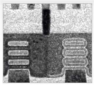
TSMC has new transistor structure (nanosheet) and new materials such as high mobility channel, 2D, carbon nanotube (CNT). TSMC has already demonstrated at 32Mb nanosheet SRAM fully-functional at 0.46V. It has also identified promising 2D materials such as MoS2 (molybdenum disulfide). At IEDM last year, they disclosed the first BEOL CNT power-gating device integrated with silicon-based CMOS.
Scaling continues with EUV advances with the current generation of scanners. They are also working with ASML (the only supplier of EUV equipment) on High-NA EUV [read more...]


Aug 27, 2020

Chip in the Fields: SBCCI and SBMicro Conferences

Chip in the Fields
C̶a̶m̶p̶i̶n̶a̶s̶,̶ ̶S̶P̶,̶ ̶B̶r̶a̶z̶i̶l̶ ̶ 
Virtual
August 24 to 28, 2020

Due to the COVID-19 pandemic the Chip in the Fields is changed to a virtual event. In 2021 we plan to have again the normal live Chip in the Fields events to be held in Hotel Premium, Campinas, SP, Brazil

The conferences SBCCI and SBMicro started in the early 80’s and since the year 2000 they joined forces, organizing them at the same venue and under a unified fantasy name “Chip in Somewhere”. The somewhere could be the name of the city or a fantasy name related to the region. It started with the name of “Chip in the Jungle”, because it was held in Manaus, the heart of the Amazon forest. 

Along these 21 years of Chip in, gradually other conferences joined the common venue and organization. Nowadays, we are composed of five sister conferences: SBCCI, SBMicro, WCAS, INSCIT and Sforum, as described in the respective call for papers. Due to the COVID-19 pandemic the Chip in the Fields is changed to a virtual event. Detalhes of the program and access link will be made available in the near future. Please follow the conference website for future up-dates.

Keynote Speakers

Kenneth K. O

Texas Analog Center of Excellence and Dept. of ECE,
The University of Texas at Dallas, Richardson, TX

Rajiv V. JoshiT. J. Watson research center, IBM                                         


Sponsored by:

Co-sponsored by:

Organized by:

Supported by:

Silicon Sponsors:

Platinum Sponsors:

Silver Sponsors:


Events: