Showing posts with label mosfet. Show all posts

Jun 10, 2020

[paper] Nanowire gate-all-around MOSFETs modeling

Cheng, He, Tiefeng Liu, Chao Zhang, Zhijia Yang, Zhifeng Liu, Kazuo Nakazato
and Zhipeng Zhang
Nanowire gate-all-around MOSFETs modeling:
ballistic transport incorporating the source-to-drain tunneling
Japanese Journal of Applied Physics (2020)
Accepted Manuscript online 5 June 2020
DOI: 10.35848/1347-4065/ab99db

Abstract: Incorporating the source-to-drain tunneling current valid in all operating regions, an analytical compact model is proposed for cylindrical ballistic GAA-nMOSFETs with ultra-short Silicon channel. From taking the DIBL effect into consideration, the potential distribution within the device channel has been modeled based upon a 2-D analysis in our previous work. In this study, by introducing a parabolic function when modeling the potential profile in the channel direction, we found out that the source-to-drain tunneling effect in the subthreshold region could be evaluated analytically by applying WKB approximation. Then, it is practical to estimate the drain current for all operating regions analytically with this compact model considering both the source-to-drain tunneling and thermionic transport. The resulting analytic compact model is tested against NEGF simulation using SILVACO, and good accuracy is demonstrated. Finally, we perform an NMOS inverter circuit simulation using HSPICE, introducing our model to it as a Verilog-A script.

Fig: Rough sketch of the potential energy profile along the channel and illustration of mechanisms governing the carrier transport in ballistic tunneling and thermionic modes.
(a) Representation of energy levels distribution along the z-direction at the channel center (r = 0).
(b) Schematics of confinement potential energy distribution along r-component at the barrier top (z = zMAX) in the cross section. The elementary charge stands for letter e. 

Acknowledgment: The authors would like to thank Prof. S. Uno for his support to this work. This work has been supported by the science and technology program of Liaoning, the major industrial projects (Grant No. 2019JH1/1010022


May 26, 2020

[paper] InAs-OI-Si MOSFET Compact Model

S. K. Maity, A. Haque and S. Pandit
Charge-Based Compact Drain Current Modeling of InAs-OI-Si MOSFET 
Including Subband Energies and Band Nonparabolicity
in IEEE TED, vol. 67, no. 6, pp. 2282-2289, June 2020
doi: 10.1109/TED.2020.2984578

Abstract: In this article, we report a physics-based compact model of drain current for InAs-on-insulator MOSFETs. The quantum confinement effect has been incorporated in the proposed model by solving the 1-D Schrödinger–Poisson equations without using any empirical model parameter. The model accurately captures the variation of surface potential, charge density in the inversion layer, and subband energy levels with gate bias inside the quantum well. The conduction-band nonparabolicity effect on modification in eigen energy, effective mass, and density of states is derived and incorporated into the proposed model. The velocity overshoot effect that originates from the quasi-ballistic nature of carrier transport is also considered in the model. The proposed drain current model has been implemented in Verilog-A to use in the SPICE environment. The model predicted results are in good agreement with the commercial device simulator results and experimental data. 
Fig: Energy band profile of InAs-OI-Si MOSFET in the direction perpendicular to the oxide interface at flat-band condition. E0 and E1 denote the first and the second subband energy levels, respectively, and ΔEc and Vox represent the conduction-band offset between buffer-channel and oxide-channel regions, respectively.

Acknowledgment: The author S. Pandit would like to thank the Department of Electronics and Information Technology, Government of India for utilizing the resources obtained under the SMDP-C2SD Project at the University of Calcutta.

URL: https://ieeexplore.ieee.org/stamp/stamp.jsp?tp=&arnumber=9067014&isnumber=9098120

May 5, 2020

[paper] Two Transistors Voltage-Measurement-Based Test Structure for Fast MOSFET Device Mismatch Characterization

J. P. M. Brito and S. Bampi
Two Transistors Voltage-Measurement-Based Test Structure 
for Fast MOSFET Device Mismatch Characterization
IEEE Transactions on Semiconductor Manufacturing
doi: 10.1109/TSM.2020.2988095

Abstract - This work presents a test structure targeted to measure MOSFET mismatches with a fast method. It relies on two single-spot voltage measurements in order to extract VTH and β/β separately. The new methodology gives a theoretical increase in the measurement speed of 30x (23.17x in practice). The coefficient of determination (R2) of the linear regression analysis is used to compare standalone transistor measurements against the new proposed methodology. The correlation in the data demonstrates values not less than 0.94 (R2≥ 0.94). The test structure can reproduce parameter correlations, and it is capable of extracting MOSFET mismatch design parameters, such as Pelgrom’s AVTH, with an error of 2% and Aβ, with a negligible error. The experimental data presented herein are taken from measurements in prototypes fabricated in a 65nm CMOS bulk process. The whole circuit is composed of 16 2D addressable DUT device matrices, each having 256 same-size closely-placed MOSFET devices, totaling 4,096 MOS devices used in single-type (NMOS) transistor array. 

URL: https://ieeexplore.ieee.org/stamp/stamp.jsp?tp=&arnumber=9068274&isnumber=5159394

May 4, 2020

[paper] Benchmark Tests for MOSFET Thermal Noise Models

Scholten A.J., Smit G.D.J., Pijper R.M.T., Tiemeijer L.F.
Benchmark Tests for MOSFET Thermal Noise Models
In: Grasser T. (eds) Noise in Nanoscale Semiconductor Devices. Springer, Cham

Abstract - In today’s semiconductor industry, many traditional integrated device manufacturers (IDMs) are moving away from chip manufacturing, and transforming into fabless companies that use foundry services for manufacturing their ICs. This is especially true in the field of advanced CMOS technologies. In these companies-under-transformation, the work of the modeling engineer is changing: instead of building models from scratch themselves, most companies choose to use the modeling packages that are delivered by the foundries. There are two reasons to be skeptical about RF noise models. First, measurement of noise, and RF noise in particular, is a difficult and specialist topic. One should not take for granted that every company has the required expertise to carry out this task successfully. A second reason to check RF noise models is that the most popular compact MOSFET models are BSIM4 [1] and BSIMBULK [2], which are not particularly strong and certainly not predictive when it comes to RF noise. As a consequence, the work of the modeling engineer is changing from model creation to model verification.

Tab: Overview of benchmark tests for thermal noise
#No
Bias
Length
Quantity
Test
Remark
#1
VDS = 0V
All
SID
γ = 1

#2
VDS = 0 V
All
SIG
β = 5/12

#3
VDS = 0 V
All
c
c = 0
In the limit f ↓ 0 Hz
#4
Weak Inv
All
SID
F = 1
Disregard SIG contributions from gate to drain
#5
Saturation
Long
SID
γ = 2/3

#6
Saturation
Long
SIG
β = 4/3

#7
Saturation
Long
c
c = 0.4j

#8
Saturation
Short
SID
γ enhancement
Switch off gate resistance
#9
Saturation
All
SID
γ D,NMOS ≥ γ D,PMOS
Switch off gate resistance
#10
Saturation
All
SID
Different Vth flavors should nearly coincide
When plotted against ID


First Online: 27 April 2020
DOI: 10.1007/978-3-030-37500-3_20

Ref: 
[1] N. Paydavosi, T.H. Morshed, D.D. Lu, W. Yang, M.V. Dunga, X. Xi, J. He, W. Liu, K.M. Cao, X. Jin, J.J. Ou, M. Chan, A.M. Niknejad, C. Hu, BSIM4v4.8.0 MOSFET Model - User’s Manual. [Online]. Available: http://bsim.berkeley.edu/models/bsim4/
[2] H. Agarwal, C. Gupta, H.-L. Chang, S. Khandelwal, J.P. Duarte, Y.S. Chauhan, S. Salahuddin, C. Hu, BSIM-BULK106.2.0 MOSFET Compact Model - Technical Manual. [Online]. Available: http://bsim.berkeley.edu/models/bsimbulk/

May 1, 2020

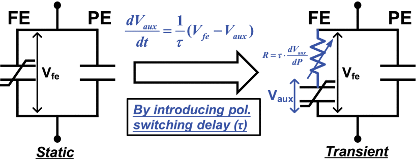
[paper] Physical Mechanisms of Reverse DIBL and NDR in FeFETs With Steep Subthreshold Swing

C. Jin, T. Saraya, T. Hiramoto and M. Kobayashi,
in IEEE J-EDS, vol. 8, pp. 429-434, 2020
doi: 10.1109/JEDS.2020.2986345

Abstract - We have investigated transient IdVg and IdVd characteristics of ferroelectric field-effect transistor (FeFET) by simulation with ferroelectric model considering polarization switching dynamics. We show transient negative capacitance (TNC) with polarization reversal and depolarization effect can result in sub-60mV/dec subthreshold swing (SS), reverse drain-induced barrier lowering (R-DIBL), and negative differential resistance (NDR) without traversing the quasi-static negative capacitance (QSNC) region of the S-shaped polarization-voltage (PV) predicted by single-domain Landau theory. Moreover, the mechanisms of R-DIBL and NDR based on the TNC theory are discussed in detail. The results demonstrated in this work can be a possible explanation for the mechanism of previously reported negative capacitance field-effect transistor (NCFET) with sub-60mV/dec SS, R-DIBL, and NDR.
Equivalent circuits of a ferroelectric capacitor in both static and transient conditions.

Apr 24, 2020

Online Classes on The Principle of Semiconductor Devices

Professor Mansun Chan, UST (HK), has developed a 13 weeks online class on the principle of semiconductor devices.  Unlike tradition lectures, the class use extensive animations to help students to visualize the actions of carriers in a device.  The classes was divided into two part, part I on semiconductor carrier statistics, PN Junction, BJT and part II on MOSFET and advanced FET.


Meet your instructor:

Mansun Chan
Chair Professor, Department of Electronic and Computer Engineering
The Hong Kong University of Science and Technology


conference FOSS paper reached 300 reads


D. Tomaszewski, G. Głuszko, M. Brinson, V. Kuznetsov and W. Grabinski, "FOSS as an efficient tool for extraction of MOSFET compact model parameters," 2016 MIXDES - 23rd International Conference Mixed Design of Integrated Circuits and Systems, Lodz, 2016, pp. 68-73.

Abstract - A GNU Octave - based application for device-level compact model evaluation and parameter extraction has been developed. The applications main features are as follows: experimental I–V data importing, generating input data for different circuit simulation programs, running the simulation program to calculate I–V characteristics of the specified models, calculating model misfit and its sensitivity to selected parameter variation, and the comparison of experimental and simulated characteristics. Measured I–V data stored by different measurement systems are accepted. Circuit simulations may be done with Ngspice, Qucs and LTSpiceIV © . Selected aspects of the application are presented and discussed.

Apr 14, 2020

ICMTS2020 #paper: Cutoff Frequency Fluctuation in RF-MOSFETs

2020 ICMTS, April 6-9, Edinburgh (UK)
Novel Statistical Modeling and Parameter Extraction Methodology
of Cutoff Frequency for RF-MOSFETs
Chika Tanaka, Yasuhiko Iguchi, Atsushi Sueoka, and Sadayuki Yoshitomi
Memory Division, Kioxia Corporation
2-5-1, Kasama, Sakae-ku, Yokohama, 247-8585, Japan

Abstract: The cutoff frequency fluctuation in RF-MOSFET has been investigated. Detailed analysis for capacitance fluctuation as well as the extraction of an intrinsic MOSFET parameter were performed. The extracted process parameters were verified by the framework of effective mobility. The global statistical model of cutoff frequency was successfully developed in terms of capacitance fluctuation, considering intrinsic (channel and bulk charge) and extrinsic (overlap and fringe) capacitance components separately and identifying the major variability sources for cutoff frequency by using extracted parameter.
Fig: Calculated σfT is plotted against σfT obtained from measured data.


Mar 30, 2020

conference paper reached 700 reads

M. Bucher, A. Bazigos and W. Grabinski, "Determining MOSFET Parameters in Moderate Inversion," 2007 IEEE Design and Diagnostics of Electronic Circuits and Systems, Krakow, 2007, pp. 1-4.

Abstract: Deep submicron CMOS technology scaling leads to reduced strong inversion voltage range due to non-scalability of threshold voltage, while supply voltage is reduced. Moderate inversion operation therefore becomes increasingly important. In this paper, a new method of determining MOSFET parameters in moderate inversion is presented. Model parameters are determined using a constant current bias technique, where the biasing current is estimated from the transconductance-to-current ratio. This technique is largely insensitive to mobility effects and series resistance. Statistical data measured on 40 dies a 0.25 um standard CMOS technology are used for the illustration of this method.

Mar 23, 2020

MicroTec: Semiconductor Process and Device Simulator

Software Package for 2D Process and Device Simulation
Version 4.0 for Windows
User’s Manual
Publisher: Siborg Systems Inc
Editor: Michael S. Obrecht

MicroTec allows 2D silicon process modeling including implantation, diffusion and oxidation and 2D steady-state semiconductor device simulation like MOSFET, DMOS, JFET, BJT, IGBT, Schottky, photosensitive devices etc. Although MicroTec is significantly simplified compared to widely available commercial simulators, it nevertheless is a very powerful modeling tool for industrial semiconductor process/device design. In many instances MicroTec outperforms existing commercial tools and it is remarkably robust and easy-to-use.

FIG: MicroTec SibGraf GUI windows


Jan 9, 2019

Compact Transcapacitance Model for Short Channel DG FinFETs

(Proceedings of the Int. Conference on Microwave and THz Technologies and Wireless Comm.)
Ashkhen Yesayan
Institute of Radiophysics and Electronics
Alikhanian Brothers str. 1, 0203 Ashtarak, Armenia
Received 15 November 2018

Abstract: A compact capacitance model is developed accounting for small-geometry effects in FinFETs. While decreasing the channel length, the transcapacitance model becomes very sensitive to all short channel effects, both in moderate and strong inversion regimes. In addition, for short channel devices, we need to take into account the inter-electrode capacitive coupling in the subthreshold regime, which is not significant for long channel devices. The quantum mechanical effects, which are very significant for thin Fins, are included in the model. The effect of mobility degradation on C-V characteristics is also demonstrated. The model was validated with numerical 3D Atlas simulations and a good accuracy of the model has been demonstrated in all operating regimes.

References:
[1] Tech. rep., International technology roadmap for semiconductor (ITRS). 2009.
[2] J.-M. Sallese, F. Krummenacher, F. Pregaldiny, C. Lallement, A. Roy, C. Enz, A design oriented charge-based current model for symmetric DG MOSFET and its correlation with the EKV formalism, Solid-State Electron, vol. 49 no. 3, pp. 485–489. 2005.
[3] A Yesayan, F Prégaldiny, N Chevillon, C Lallement, JM Sallese, Physics-based compact model for ultra-scaled FinFETs, Solid-State Electronics, vol. 62, no1, pp. 165-173, 2011.
[4] Liang X, Taur Y., A 2-D analytical solution for SCEs in DG MOSFETs. IEEE Trans Electron Dev 2004;51(9):1385–91.
[5] Ward D, Dutton R. ,A charge-oriented model for MOS transistor capacitances. IEEE J Solid-State Circ, 1978;13(5):703–8.
[6] Tang M. Etude et modélisation compacte du transistor FinFET. Ph.D. Thesis, University of Strasbourg; December 2009.
[7] Borli H, Vinkenes K, Fjeldly T., Physics-based capacitance modeling of short-channel double-gate MOSFETs. Phys Status Solidi (c) 2008;5(12):3643–6.
[8] Arora N., MOSFET models for VLSI circuit simulation. New York: Theory and Practice, Springer-Verlag; 1993, ISBN:3-211-82395-6

Source:

Feb 28, 2018

[paper] Compact electro-thermal modeling of a SiC MOSFET power module under short-circuit conditions

Proceedings of 43rd Annual Conference of the IEEE Industrial Electronics Society
IECON 2017
Lorenzo Ceccarelli, Paula Diaz Reigosa, Amir Sajjad Bahman, Francesco Iannuzzo,
Frede Blaabjerg
Center of Reliable Power Electronics, Department of Energy Technology Aalborg University,
Pontoppidanstræde 101
9220 Aalborg, Denmark 

ABSTRACT: A novel physics-based, electro-thermal model which is capable of estimating accurately the short-circuit behavior and thermal instabilities of silicon carbide MOSFET multi-chip power modules is proposed in this paper. The model has been implemented in PSpice and describes the internal structure of the module, including stray elements in the multi-chip layout, self-heating effect, drain leakage current and threshold voltage mismatch. A lumped-parameter thermal network is extracted in order to estimate the internal temperature of the chips. The case study is a half-bridge power module from CREE with 1.2 kV breakdown voltage and about 300 A rated current. The short-circuit behavior of the module is investigated experimentally through a non-destructive test setup and the model is validated. The estimation of overcurrent and temperature distribution among the chips can provide useful information for the reliability assessment and fault-mode analysis of a new-generation SiC high-power modules [read more...]

Fig.: SiC MOSFET model structure. 

Nov 3, 2017

[paper] Validation of MOSFET Model Source–Drain Symmetry

Validation of MOSFET Model Source-Drain Symmetry
Colin C. McAndrew
IEEE TED, Vol. 53, No. 9, Sep. 2006
doi: 10.1109/TED.2006.881005

Abstract: Symmetry around Vds= 0 is a critical requirement for MOSFET models, e.g. as it affects the ability of a model to simulate distortion accurately for some RF CMOS mixers. The Gummel symmetry test (GST) has been the standard test used to evaluate the symmetry of MOSFET models. However, this test is only applicable to DC current, and is only valid when there is negligible gate or substrate current. This paper presents a DC symmetry test that is applicable in the presence of gate and substrate currents, and an AC symmetry test that is simple and effective in verifying symmetry of Cgs and Cgd.


FIG: Biasing scheme for dc symmetry testing. 

Sep 12, 2017

[book] Systematic Design of Analog CMOS Circuits

Paul G. A. Jespers, Boris Murmann
Cambridge University Press; 31 Oct 2017; 342pp

Discover a fresh approach to efficient and insight-driven analog integrated circuit design in nanoscale-CMOS with this hands-on guide. Expert authors present a sizing methodology that employs SPICE-generated lookup tables, enabling close agreement between hand analysis and simulation. This enables the exploration of analog circuit tradeoffs using the gm/ID ratio as a central variable in script-based design flows, and eliminates time-consuming iterations in a circuit simulator. Supported by downloadable MATLAB code, and including over forty detailed worked examples, this book will provide professional analog circuit designers, researchers, and graduate students with the theoretical know-how and practical tools needed to acquire a systematic and re-use oriented design style for analog integrated circuits in modern CMOS.

Aug 3, 2017

Basics of MOSFET Modeling


Basics of MOSFET Modeling with LabVIEW/LTspice 
  • Introduction to MOSFET Models 
  • Functions and Parameter Extraction
  • visit http://mosfet-engineer.blogspot.com

Aug 1, 2017

[paper] Circuit-level simulation methodology for Random Telegraph Noise by using Verilog-AMS


T. Komawaki, M. Yabuuchi, R. Kishida, J. Furuta, T. Matsumoto and K. Kobayashi
Circuit-level simulation methodology for Random Telegraph Noise by using Verilog-AMS
2017 IEEE ICICDT, Austin, TX, USA, 2017, pp. 1-4.
doi: 10.1109/ICICDT.2017.7993526

Abstract: As device sizes are downscaled to nanometer, Random Telegraph Noise (RTN) becomes dominant. It is indespensable to accurately estimate the effect of RTN. We propose the RTN simulation method for analog circuits. It is based on the charge trapping model. We replicate the RTN-induced threshold voltage fluctuation to attach a variable DC voltage source to the gate of MOSFET by using Verilog-AMS. We confirm that drain current of MOSFETs temporally fluctuates. The fluctuations of RTN are different for each MOSFET. Our proposed method can be applied to estimate the temporal impact of RTN including multiple transistors. We can successfully replicate RTN-induced frequency fluctuations in 3-stage ring oscillators as similar as the measurement results [read more...]

Jul 26, 2017

[paper] A Compact Model for the Statistics of the Low-Frequency Noise of MOSFETs With Laterally Uniform Doping

M. Banaszeski da Silva, H. P. Tuinhout, A. Zegers-van Duijnhoven, G. I. Wirth and A. J. Scholten
"A Compact Model for the Statistics of the Low-Frequency Noise of MOSFETs With Laterally Uniform Doping" 
in IEEE TED, vol. 64, no. 8, pp. 3331-3336, Aug. 2017.
doi: 10.1109/TED.2017.2713301

Abstract: In this paper, we develop a compact physics-based statistical model for random telegraph noise-related low-frequency noise in bulk MOSFETS with laterally uniform doping. The proposed model is suited for modern compact device models, such as PSP, BSIM, and EKV. With our proposed model, one can calculate the expected value and the variability of the noise as a function of bias and device parameters. We validate the model through numerous experimental results from different CMOS nodes, down to 40 nm [read more...]

Jul 25, 2017

[paper] Compact On-Wafer Test Structures for Device RF Characterization

B. Kazemi Esfeh, K. Ben Ali and J. P. Raskin IEEE Fellow
Compact On-Wafer Test Structures for Device RF Characterization
in IEEE TED, vol. 64, no. 8, pp. 3101-3107, Aug. 2017
doi: 10.1109/TED.2017.2717196

Abstract: The main objective of this paper is to validate the radio frequency (RF) characterization procedure based on compact test structures compatible with 50um pitch RF probes. It is shown that by using these new test structures, the layout geometry and hence the on-chip space consumption for complete sets of passive and active devices, e.g., coplanar waveguide transmission lines and RF MOSFETs, is divided by a factor of two. The validity domain of these new compact test structures is demonstrated by comparing their measurement results with classical test structures compatible with 100–150um pitch RF probes. 50um -pitch de-embedding structures have been implemented on 0.18um RF silicon-on-insulator (SOI) technology. Cutoff frequencies and parasitic elements of the RF SOI transistors are extracted and the RF performance of trap-rich SOI substrates is analyzed under small- and large-signal conditions [read more...]


Jul 4, 2017

[paper] A Compact Model for the Statistics of the Low-Frequency Noise of MOSFETs With Laterally Uniform Doping

A Compact Model for the Statistics of the Low-Frequency Noise of MOSFETs With Laterally Uniform Doping
M. Banaszeski da Silva; H. P. Tuinhout; A. Zegers-van Duijnhoven; G. I. Wirth; A. J. Scholten;
in IEEE Transactions on Electron Devices, vol.PP, no.99, pp.1-6
doi: 10.1109/TED.2017.2713301

Abstract: In this paper, we develop a compact physics-based statistical model for random telegraph noise-related low-frequency noise in bulk MOSFETS with laterally uniform doping. The proposed model is suited for modern compact device models, such as PSP, BSIM, and EKV. With our proposed model, one can calculate the expected value and the variability of the noise as a function of bias and device parameters. We validate the model through numerous experimental results from different CMOS nodes, down to 40 nm. [read more...]

Feb 7, 2017

[paper] Impact of technology scaling on analog and RF performance of SOI–TFET

Impact of technology scaling on analog and RF performance of SOI–TFET
P Kumari, S Dash and G P Mishra
Advances in Natural Sciences: Nanoscience and Nanotechnology, Volume 6, Number 4 
Published 9 October 2015

Abstract
This paper presents both the analytical and simulation study of analog and RF performance for single gate semiconductor on insulator tunnel field effect transistor in an extensive manner. Here 2D drain current model has been developed using initial and final tunneling length of band-to-band process. The investigation is further extended to the quantitative and comprehensive analysis of analog parameters such as surface potential, electric field, tunneling path, and transfer characteristics of the device. The impact of scaling of gate oxide thickness and silicon body thickness on the electrostatic and RF performance of the device is discussed. The analytical model results are validated with TCAD Sentaurus device simulation results [read more...]

Citations
[1] Extensive electrostatic investigation of workfunction-modulated SOI tunnel FETs Subhrasmita Panda et al  2016 Journal of Computational Electronics 15 1326
[2] S. Sahoo et al  2016 337
[3] A comprehensive investigation of silicon film thickness (T SI) of nanoscale DG TFET for low power applications Rajeev Ranjan et al  2016 Advances in Natural Sciences: Nanoscience and Nanotechnology 7 03500
[4] A complete analytical potential based solution for a 4H-SiC MOSFET in nanoscale M K Yadav et al  2016 Advances in Natural Sciences: Nanoscience and Nanotechnology 7 025011
[5] S. Dash et al  2015 447