Showing posts with label Logic gates. Show all posts

Apr 3, 2024

[paper] CMOS Technology for Analog Applications in High Energy Physics

Gianluca Traversi, Luigi Gaioni, Lodovico Ratti, Valerio Re and Elisa Riceputi
Characterization of a 28 nm CMOS Technology
for Analog Applications in High Energy Physics 
in IEEE Transactions on Nuclear Science
DOI: 10.1109/TNS.2024.3382348

1 INFN Pavia and Dipartimento di Ingegneria e Scienze Applicate, Uni. Bergamo, Italy
2 INFN Pavia and Dipartimento di Ingegneria Industriale e dell’Informazione, Uni. Pavia, Italy

Abstract: In the last few years, the 28 nm CMOS technology has raised interest in the High Energy Physics community for the design and implementation of readout integrated circuits for high granularity position sensitive detectors. This work is focused on the characterization of the 28 nm CMOS node with a particular focus on the analog performance. Small signal characteristics and the behavior of the white and 1/f noise components are studied as a function of the device polarity, dimensions, and bias conditions to provide guidelines for minimum noise design of front-end electronics. Comparison with data extracted from previous CMOS generations are also presented to assess the performance of the technology node under evaluation. 

Fig: Transconductance efficiency gm/ID as a function of the normalized
drain current IDL/W for NMOS (a) and PMOS (b) devices (|VDS| = 0.9 V)


Acknowledgment: The activity leading to the results presented in this paper was carried out in the framework of the Falaphel project, funded by the Italian Institute for Nuclear Physics (INFN). The authors wish to thank Prof. Massimo Manghisoni (University of Bergamo) for the valuable advice which contributed to improve this work and Dr. Stefano Bonaldo (University of Padova) for fruitful discussions on the measurement results. The authors wish to thank also Barbara Pini (INFN Torino) for the wire bonding of the chips, Emilio Meroni and Nicola Cattaneo (University of Bergamo) for the characterization activity.


Jan 8, 2024

[paper] Polylogarithms in MOSFET Modeling

A. Ortiz-Conde and F. J. García-Sánchez
Recent Applications of Polylogarithms in MOSFET Modeling
2023 IEEE 33rd International Conference on Microelectronics
MIEL, Nis, Serbia, 2023, pp. 1-8
DOI: 10.1109/MIEL58498.2023.10315897

Department of Electronics and Circuits, Universidad Simón Bolívar, Caracas, Venezuela

Abstract: We present a review of recent uses of the special mathematical function known as the polylogarithm for MOSFET modeling applications. We first summarize some basic properties of polylogarithms, with a particular focus on those with negative exponential argument. After examining cases of the use of first order polylogarithms pertinent to electron device modeling, we explain the reasons that motivate the use of polylogarithms of diverse orders for formulating mono- and poly-crystalline succinct compact MOSFET models. We then analyze a particular representative example: the modeling of polysilicon MOSFETs using the polylogarithm. Recalling that polylogarithms may be used to faithfully represent Fermi-Dirac Integrals in general, and considering that they are analytically differentiable and integrable, we describe a full Fermi–Dirac Statistics-based version of the usually approximate Boltzmann Statistics-based MOSFET Surface Potential Equation (SPE).

TABLE: Some Features of Polylogarithms with Negative Exponential Argument


Mar 8, 2023

[paper] Cryogenic Characteristics of InGaAs MOSFET

L. Södergren, P. Olausson and E. Lind
Cryogenic Characteristics of InGaAs MOSFET
in IEEE TED, vol. 70, no. 3, pp. 1226-1230, March 2023,
DOI: 10.1109/TED.2023.3238382

Abstract: We present an investigation of the temperature dependence of the current characteristic of a long-channel InGaAs quantum well MOSFET. A model is developed, which includes the effects of band tail states, electron concentration-dependent mobility, and interface trap density to accurately explain the measured data over all modes of operation. The increased effect of remote impurity scattering is associated with mobility degradation in the subthreshold region. The device has been characterized down to 13 K, with a minimum inverse subthreshold slope of 8 mV/dec and a maximum ON-state mobility of 6700 cm2/Vs and with values of 75 mV/dec and 3000 cm2/Vs at room temperature.

FIG: Measured transfer characteristics at 13, 100, and 300 K together with the fit model with
(a) VDS=50 mV and (b) VDS=500 mV.


Nov 7, 2021

[paper] 3nm Nano-Sheet FETs

Etienne SICARD* and Lionel TROJMAN**
Introducing 3-nm Nano-Sheet FET technology in Microwind
hal-03377556: Submitted on 14 Oct 2021

  
*INSA-Dgei, Toulouse (F)
**ISEP, Issy les Moulineaux (F)


Abstract: This paper describes the implementation of the novel Nano-sheet FET (NS-FET) for the 3-nm CMOS technology node in Microwind. After a general presentation of the electronic market and the roadmap to the atomic scale, design rules and basic metrics for the 3-nm node are presented. Concepts related to the design of NS-FET and design for manufacturing are also described. The performances of a ring oscillator, basic cells, sequential cells and a 6-transistor RAM memory are also analyzed.
Fig: A simple 3-stage ring oscillator based on compiled inverters “Fast” mode.

[ref] MICROWIND software allows the designer to simulate and design an integrated circuit at physical description level. Born in Toulouse (France), Microwind is an innovative CMOS design tool for educational market.

Jun 1, 2020

[paper] Device Scaling for 3-nm Node and Beyond

Opportunities in Device Scaling for 3-nm Node and Beyond:
FinFET Versus GAA-FET Versus UFET
U. K. Das and T. K. Bhattacharyya
in IEEE TED, vol. 67, no. 6, pp. 2633-2638, June 2020, 
doi: 10.1109/TED.2020.2987139

Abstract: The performances of FinFET, gate-all-around (GAA) nanowire/nanosheet, and U-shaped FETs (UFETs) are studied targeting the 3-nm node (N3) and beyond CMOS dimensions. To accommodate a contacted gate pitch (CGP) of 32 nm and below, the gate length is scaled down to 14 nm and beyond. While going from 5-nm node (N5) to 3-nm node (N3) dimensions, the GAA-lateral nanosheet (LNS) shows 8% reduction in the effective drain current (Ieff) due to an enormous rise in short channel effects, such as subthreshold slope (SS) and drain-induced barrier lowering (DIBL). On the other hand, 5-nm diameter-based lateral nanowire shows an 80% rise in Ieff. Therefore, to enable future devices, we explored electrostatics and Ieff in FinFET, GAA-FET, and UFET architectures at a scaled dimension. The performances of both Si- and SiGe-based transistors are compared using an advanced TCAD device simulator.

Fig: Transistor architectures for future technologies. (a) FinFET device
(in {001} substrate plane, and sidewalls are in {110} planes) with crosssectional
fin channel (5 nm thin). (b) Fin is changed into a four-stacked
GAA-LNWs. (c) GAA- LNS having 20-nm width (W). (d) UFET structure.

Acknowledgment: The authors would like to thank Dr. Bidhan Pramanik, IIT Goa, India, Dr. KB Jinesh, IIST, Trivandrum, India, and Dr. Geert Eneman, IMEC, Leuven, Belgium, for their valuable technical support.

URL: https://ieeexplore.ieee.org/stamp/stamp.jsp?tp=&arnumber=9078841&isnumber=9098120

May 1, 2020

[paper] Physical Mechanisms of Reverse DIBL and NDR in FeFETs With Steep Subthreshold Swing

C. Jin, T. Saraya, T. Hiramoto and M. Kobayashi,
in IEEE J-EDS, vol. 8, pp. 429-434, 2020
doi: 10.1109/JEDS.2020.2986345

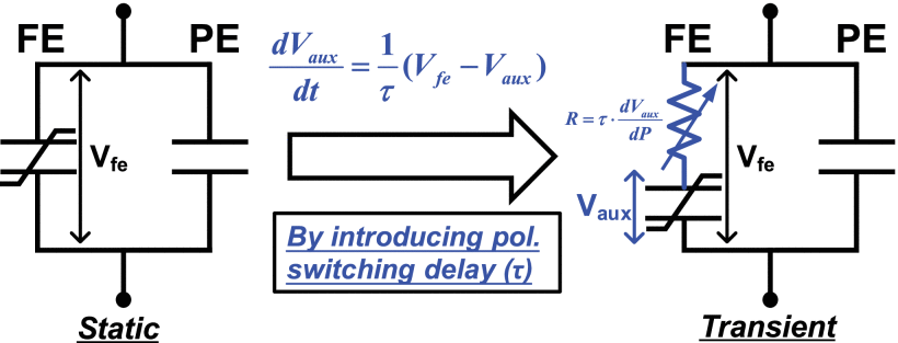
Abstract - We have investigated transient IdVg and IdVd characteristics of ferroelectric field-effect transistor (FeFET) by simulation with ferroelectric model considering polarization switching dynamics. We show transient negative capacitance (TNC) with polarization reversal and depolarization effect can result in sub-60mV/dec subthreshold swing (SS), reverse drain-induced barrier lowering (R-DIBL), and negative differential resistance (NDR) without traversing the quasi-static negative capacitance (QSNC) region of the S-shaped polarization-voltage (PV) predicted by single-domain Landau theory. Moreover, the mechanisms of R-DIBL and NDR based on the TNC theory are discussed in detail. The results demonstrated in this work can be a possible explanation for the mechanism of previously reported negative capacitance field-effect transistor (NCFET) with sub-60mV/dec SS, R-DIBL, and NDR.
Equivalent circuits of a ferroelectric capacitor in both static and transient conditions.