Nov 16, 2017

Innovations in Electronics and Communication Engineering

Proceedings of the Fifth ICIECE 2016
Volume 7 of Lecture Notes in Networks and Systems
H. S. Saini, R. K. Singh, K. Satish Reddy
Springer, 8 Nov 2017 - Technology & Engineering - 596 pages
ISBN 9811038120, 9789811038129

The book contains high quality papers presented in the Fifth International Conference on Innovations in Electronics and Communication Engineering (ICIECE 2016) held at Guru Nanak Institutions, Hyderabad, India during 8 and 9 July 2016. The objective is to provide the latest developments in the field of electronics and communication engineering specially the areas like Image Processing, Wireless Communications, Radar Signal Processing, Embedded Systems and VLSI Design. The book aims to provide an opportunity for researchers, scientists, technocrats, academicians and engineers to exchange their innovative ideas and research findings in the field of Electronics and Communication Engineering [read more...]

Nov 14, 2017

The Pentagon is set to make a big push toward #opensource software next year https://t.co/EMWCKvEoQM


from Twitter https://twitter.com/wladek60

November 14, 2017 at 10:45PM
via IFTTT

3 #opensource alternatives to AutoCAD https://t.co/ysUQCGiq8X https://t.co/V68oi64jF3


from Twitter https://twitter.com/wladek60

November 14, 2017 at 10:38AM
via IFTTT

7th All-Russian Workshop on CAD of IC Design

7th All-Russian Workshop on computer aided design (CAD) of integrated circuits (IC) to be held at NRNU MEPhI on December 12-14, 2017. The free workshop is organized by NRNU MEPhI jointly with Cadence Design Systems. The program and further information about the Workshop is available via site cad.mephi.ru.

Program 
(with timetable and detailed information in pdf format)
12 December 2017
08:45 - 09:15Registration (University entrance)
09:30 - 13:00Conference hall 3rd floor of the main lecture building
- Synthesis in Genus (28nm technology)
- Introduction to Joules
- Innovus 17.1 Topical Introduction
13:00 - 14:00
Lunch break
14:00 - 18:15Conference hall 3rd floor of the main lecture building
- Introduction to Stylus
- Physical verification with the help of PVS
- A new generation of verification software - Xcelium and Indago
- The history and future of megatrends in EDA
13 December 2017
9:00 - 18:00
Laboratory V-315 of the Department of Electronics
(Practical classes)
- Behavioral modeling
- Logical synthesis
- Simulation of a Verilog modules with element delays
- Physical design of the digital modules
- Verification of the digital modules
14 December 2017


10:00 - 12:00Laboratory V-315 of the Department of Electronics
- Working discussions, summarizing

Contact Event Secretary: E. Atkin
+7 495 7885699 ext. 9155
+7 499 3242597

Nov 11, 2017

#paper A temperature‐dependent surface potential‐based algorithm for extraction of Vth in homojunction TFETs https://t.co/uhg1laMLY2


from Twitter https://twitter.com/wladek60

November 11, 2017 at 07:15PM
via IFTTT

#Tesla-inspired Chinese EV startup launches all-electric SUV using #opensource patents https://t.co/LYByI2RCyr


from Twitter https://twitter.com/wladek60

November 11, 2017 at 09:39AM
via IFTTT

Nov 6, 2017

A Near-Threshold Voltage Oriented Library for High-Energy Efficiency and Optimized Performance in 65nm CMOS https://t.co/OOQYhqgx9U #paper


from Twitter https://twitter.com/wladek60

November 06, 2017 at 08:26PM
via IFTTT

Nov 3, 2017

[paper] Validation of MOSFET Model Source–Drain Symmetry

Validation of MOSFET Model Source-Drain Symmetry
Colin C. McAndrew
IEEE TED, Vol. 53, No. 9, Sep. 2006
doi: 10.1109/TED.2006.881005

Abstract: Symmetry around Vds= 0 is a critical requirement for MOSFET models, e.g. as it affects the ability of a model to simulate distortion accurately for some RF CMOS mixers. The Gummel symmetry test (GST) has been the standard test used to evaluate the symmetry of MOSFET models. However, this test is only applicable to DC current, and is only valid when there is negligible gate or substrate current. This paper presents a DC symmetry test that is applicable in the presence of gate and substrate currents, and an AC symmetry test that is simple and effective in verifying symmetry of Cgs and Cgd.


FIG: Biasing scheme for dc symmetry testing. 

Nov 2, 2017

Circuit-aging #modeling based on dynamic MOSFET degradation and its verification (#SISPAD) https://t.co/QgJ5UIe7Yx


from Twitter https://twitter.com/wladek60

November 02, 2017 at 10:43AM
via IFTTT

Analytical #modeling is both science and art https://t.co/DBdMqRJqkU https://t.co/G45cufzKTb


from Twitter https://twitter.com/wladek60

November 02, 2017 at 10:07AM
via IFTTT

#Modeling of flicker noise in quasi-ballistic FETs - IEEE Conference Publication https://t.co/JpropPaK27


from Twitter https://twitter.com/wladek60

November 02, 2017 at 10:05AM
via IFTTT

Circuit-aging #modeling based on dynamic MOSFET degradation and its verification - IEEE Conference Publication https://t.co/QnZG525Y7R


from Twitter https://twitter.com/wladek60

November 02, 2017 at 10:04AM
via IFTTT

Oct 31, 2017

[mos-ak] [2nd Announcement and Call for Papers] 10th International MOS-AK Workshop in the Silicon Valley

10th International MOS-AK Workshop
(co-located with the CMC Meeting and IEDM Conference)
http://www.mos-ak.org/silicon_valley_2017/
Silicon Valley, December 6, 2017
2nd Announcement and Call for Papers 

Together with local organization teams Cadence Design Systems and Keysight Technologies as well as International MOS-AK Board of R&D Advisers: Larry Nagel, Omega Enterprises Consulting (USA), Andrei Vladimirescu, UCB (USA); ISEP (FR) and all the Extended MOS-AK TPC Committee, we have pleasure to invite to the MOS-AK Compact Modeling Workshop which will be organized for consecutive 10th time in the timeframe of coming IEDM and CMC Meetings.

Planned,10th MOS-AK workshop organized in the Silicon Valley, aims to strengthen a network and discussion forum among experts in the field, enhance open platform for information exchange related to compact/SPICE modeling and Verilog-A standardization, bring people in the compact modeling field together, as well as obtain feedback from technology developers, circuit designers, and CAD/EDA tool developers and vendors. 

Important Dates: 
  • Call for Papers - Sept. 2017
  • 2nd Announcement - Oct. 2017
  • Final Workshop Program - Nov. 2017
  • MOS-AK Workshop - Dec.6, 2017 
Venue: 
Cadence Design Systems 
2655 Seely Ave
San Jose, CA 95134
Building 5 (map)

Topics to be covered include the following among other related to the compact/SPICE modeling :
  • Compact Modeling (CM) of the electron devices
  • Advances in semiconductor technologies and processing
  • Verilog-A language for CM standardization
  • New CM techniques and extraction software
  • Open Source TCAD/EDA modeling and simulation
  • CM of passive, active, sensors and actuators
  • Emerging Devices, TFT, CMOS and SOI-based memory cells
  • Microwave, RF device modeling, high voltage device modeling
  • Nanoscale CMOS devices and circuits
  • Technology R&D, DFY, DFT and reliability/ageing IC Designs
  • Foundry/Fabless Interface Strategies
Prospective authors should submit abstract online
(any related inquiries can be sent to papers@mos-ak.org)

Online Workshop Registration
(any related inquiries can be sent to register@mos-ak.org)

Postworkshop Publications:
Selected best MOS-AK technical presentation will be recommended for further publication
in a special issue of the International Journal of High Speed Electronics and Systems

Extended MOS-AK Committee

--
You received this message because you are subscribed to the Google Groups "mos-ak" group.
To unsubscribe from this group and stop receiving emails from it, send an email to mos-ak+unsubscribe@googlegroups.com.
To post to this group, send email to mos-ak@googlegroups.com.
Visit this group at https://groups.google.com/group/mos-ak.
For more options, visit https://groups.google.com/d/optout.

[paper] Review of physics-based compact models for emerging nonvolatile memories

Nuo Xu1, Pai-Yu Chen2, Jing Wang1, Woosung Choi1, Keun-Ho Lee3, Eun Seung Jung3, Shimeng Yu2
Review of physics-based compact models for emerging nonvolatile memories
1Device Lab, Samsung Semiconductor Inc., San Jose, CA 95134, USA
2School of ECEE, Arizona State University, Tempe, AZ 85281, USA
3Semiconductor R&D Center, Samsung Electronics, Hwasung-si, Gyeonggi-do, Korea
Journal of Computational Electronics, 2017, pp. 1-13
https://doi.org/10.1007/s10825-017-1098-0

Abstract: A generic compact modeling methodology for emerging nonvolatile memories is proposed by coupling comprehensive physical equations from multiple domains (e.g., electrical, thermal, magnetic, phase transitions). This concept has been applied to three most promising emerging memory candidates: PCM, STT-MRAM, and RRAM to study their device physics as well as to evaluate their circuit-level performance. The models’ good predictability to experiments and their effectiveness in large-scale circuit simulation suggest their unique role in emerging memory research and development [read more...]

https://doi.org/10.1007/s10825-017-1098-0

SSCS Members Who Are 2017 IEEE Fellows


SSCS members who are IEEE Fellows pose with SSCS President, Jan Van der Spiegel and IEEE President, Karen Bartelson at ISSCC 2017. From left to right- Jan Van der Spiegel, Zhihua Wang, Andrei Vladimirescu, Carlo Samori, Borivoje Nikolic, Junichi Nakamura, Deog-kyoon Jeong, Hideto Hidaka, Payam Heydari, Edoardo Charbon, and Karen Bartleson 

Oct 30, 2017

How to pick a #winning #IoT #business #model https://t.co/YjMfxPAEZB https://t.co/SDOt080Ka6


from Twitter https://twitter.com/wladek60

October 30, 2017 at 03:39PM
via IFTTT

FOSDEM 2018 CAD and Open Hardware Devroom Call for Participation


This is the call for participation in the FOSDEM 2018 devroom on Computer Aided Design (CAD) tools and Open Hardware, to be held on Saturday 3 February 2018 in Brussels, Belgium. We are looking for contributions under the form of talks and tutorials covering the following main topics:
  • Printed Circuit Board (PCB) design tools (e.g. KiCad and gEDA)
  • Analogue and digital simulators (e.g. ngspice, Qucs, Gnucap, Xyce,GHDL, Icarus and Verilator)
  • Any other EDA tools such as high-level tools for digital hardware design (e.g. Migen) and HDL synthesis tools (e.g. Yosys)
  • Field solvers such as openEMS
  • Mechanical 2D and 3D CAD tools such as LibreCAD, FreeCAD, OpenSCAD andSolveSpace
  • Open Hardware projects such as the Teres laptop and the lowRISC SoC
  • Inter-project opportunities for collaboration
We hope to provide an opportunity for attendees to bring themselves up to date on the latest FOSS CAD and Open Hardware developments, share knowledge and identify opportunities to collaborate on development tasks. This devroom is an evolution of the EDA devroom we organised in 2015, 2016 and 2017.

The submission process: Please submit your proposals at

If you already have a Pentabarf account (for example as a result of having submitted a proposal in the past), make sure you use it to log in and submit your proposal. Do not create a new account if you already have one. Please provide a bit of information about yourself under Person -> Description -> Abstract. When you submit your proposal (creating an "Event" in Pentabarf), make sure you choose the "CAD and Open Hardware Devroom" in the track drop-down menu. Otherwise your proposal might go unnoticed. Fill in at least a title and abstract for the proposed talk and a suggested duration. Bear in mind that a lot of the value in these meetings comes from the discussions, so please be reasonable regarding the duration of the talk.

Important dates
  • 1 December 2017: deadline for submission of proposals
  • 8 December 2017: announcement of final schedule
  • 3 February 2018: devroom day
Recordings: The FOSDEM organisers hope to be able to live-stream and record all the talks. The recordings will be published under the same licence as all FOSDEM content (CC-BY). Only presentations will be recorded, not informal discussions and whatever happens during the lunch break. By agreeing to present at FOSDEM, you automatically give permission to be recorded. The organisers will agree to make exceptions but only for exceptional and well-reasoned cases.

Mailing list: Feel free to subscribe to the mailing list of the CAD and Open Hardware devroom to submit ideas, ask questions and generally discuss about the event:

Spread the word!

Oct 26, 2017

#Modeling the Performance of Nano Machined CMOS Transistors for Uncooled IR Sensing https://t.co/p4RnuHkJiZ


from Twitter https://twitter.com/wladek60

October 26, 2017 at 11:26AM
via IFTTT

Oct 25, 2017

UNIST Researchers Develop Highly Stable #Perovskite #Solar #Cells https://t.co/g1CN5I44r1 #paper... https://t.co/WSUSekJ1ky


from Twitter https://twitter.com/wladek60

October 25, 2017 at 08:47PM
via IFTTT

UNIST Researchers Develop Highly Stable #Perovskite #Solar #Cells https://t.co/g1CN5I44r1 #paper https://t.co/p6Jr0nPqF1


from Twitter https://twitter.com/wladek60

October 25, 2017 at 08:47PM
via IFTTT

Novel Superjunction #LDMOS (>950 V) With a Thin Layer #SOI https://t.co/1NqFJ4rAZB #paper https://t.co/LglxkaZ9PP


from Twitter https://twitter.com/wladek60

October 25, 2017 at 11:59AM
via IFTTT

Novel Superjunction #LDMOS (>950 V) With a Thin Layer #SOI https://t.co/1NqFJ4rAZB #paper


from Twitter https://twitter.com/wladek60

October 25, 2017 at 11:59AM
via IFTTT

A Planar Junctionless FET Using SiC With Reduced Impact of Interface Traps: Proposal and Analysis https://t.co/g3qPsLKIqB #paper


from Twitter https://twitter.com/wladek60

October 25, 2017 at 11:34AM
via IFTTT

Oct 24, 2017

Cryogenic characterization of CMOS technologies

A. Beckers, F. Jazaeri, A. Ruffino, C. Bruschini, A. Baschirotto and C. Enz
Cryogenic characterization of 28 nm bulk CMOS technology for quantum computing
47th ESSDERC, Leuven, Belgium, 2017, pp. 62-65.

Abstract: This paper presents the first experimental investigation and physical discussion of the cryogenic behavior of a commercial 28 nm bulk CMOS technology. Here we extract the fundamental physical parameters of this technology at 300,77 and 4.2 K based on DC measurement results. The extracted values are then used to demonstrate the impact of cryogenic temperatures on the essential analog design parameters. We find that the simplified charge-based EKV model can accurately predict the cryogenic behavior. This represents a main step towards the design of analog/RF circuits integrated in an advanced bulk CMOS process and operating at cryogenic temperature for quantum computing control systems [read more...doi: 10.1109/ESSDERC.2017.8066592


R. M. Incandela, L. Song, H. A. R. Homulle, F. Sebastiano, E. Charbon and A. Vladimirescu
Nanometer CMOS characterization and compact modeling at deep-cryogenic temperatures
47th ESSDERC, Leuven, Belgium, 2017, pp. 58-61.

Abstract: The characterization of nanometer CMOS transistors of different aspect ratios at deep-cryogenic temperatures (4 K and 100 mK) is presented for two standard CMOS technologies (40 nm and 160 nm). A detailed understanding of the device physics at those temperatures was developed and captured in an augmented MOS11/PSP model. The accuracy of the proposed model is demonstrated by matching simulations and measurements for DC and time-domain at 4 K and, for the first time, at 100 mK [read more...doi: 10.1109/ESSDERC.2017.8066591

Oct 17, 2017

A Compact QS Terminal Charge and Drain Current #Model for DG Junctionless Transistors and Its Circuit Validation https://t.co/hTsw5blL8f


from Twitter https://twitter.com/wladek60

October 17, 2017 at 11:26AM
via IFTTT

[paper] Accurate diode behavioral model with reverse recovery

Stanislav Banáša,b, Jan Divínab, Josef Dobešb, Václav Paňkoa
aON Semiconductor, SCG Czech Design Center, Department of Design System Technology, 1. maje 2594, 756 61 Roznov pod Radhostem, Czech Republic
bCzech Technical University in Prague, Faculty of Electrical Engineering, Department of Radioelectronics, Technicka 2, 166 27 Prague 6, Czech Republic
Volume 139, January 2018, Pages 31–38

Highlights:

  • The complex robust time and area scalable Verilog-A model of diode containing reverse recovery effect has been developed.
  • Due to implemented reverse recovery effect the model is useful especially for high-speed or high-voltage power devices.
  • The model can be used as stand-alone 2-terminal diode or as a parasitic p-n junction of more complex lumped macro-model.
  • Two methods of model parameter extraction or model validation have been demonstrated.

ABSTRACT: This paper deals with the comprehensive behavioral model of p-n junction diode containing reverse recovery effect, applicable to all standard SPICE simulators supporting Verilog-A language. The model has been successfully used in several production designs, which require its full complexity, robustness and set of tuning parameters comparable with standard compact SPICE diode model. The model is like standard compact model scalable with area and temperature and can be used as a stand-alone diode or as a part of more complex device macro-model, e.g. LDMOS, JFET, bipolar transistor. The paper briefly presents the state of the art followed by the chapter describing the model development and achieved solutions. During precise model verification some of them were found non-robust or poorly converging and replaced by more robust solutions, demonstrated in the paper. The measurement results of different technologies and different devices compared with a simulation using the new behavioral model are presented as the model validation. The comparison of model validation in time and frequency domains demonstrates that the implemented reverse recovery effect with correctly extracted parameters improves the model simulation results not only in switching from ON to OFF state, which is often published, but also its impedance/admittance frequency dependency in GHz range. Finally the model parameter extraction and the comparison with SPICE compact models containing reverse recovery effect is presented [read more...]

FIG: Solving the recursive calculation of reverse recovery charge

Oct 15, 2017

Oct 12, 2017

Oct 9, 2017

Intern/Student in SW Eng. for Power Management f/m

Job Description: You will be responsible for developing a SW tool enabling an user friendly and efficient framework to program system-on-chip. The flexibility of our power management solution thanks to enhanced customization is indeed a critical asset requiring a reliable tool from programming definition to release. You will be part of an enthusiastic and international system engineering team located in Munich and will get in touch locally with several design and validation teams [read more...]

Your main tasks in this full time position min 5 months up to 12 months will be to:

  • Create several functions/add-ons enhancing entry interface
  • Develop a compiler to better explore new chip architectures-Integrate compiler output with existing tools
  • Implement sanity checkers detecting
  • Develop test scenarios and requirements for chip validation
  • Contribute to the reporting and documentation for other teams and management

Oct 7, 2017

Oct 2, 2017

[paper] A Novel Reconfigurable sub-0.25V Digital Logic Family Using the Electron-Hole Bilayer TFET

Cem Alper, Jose Luis Padilla, Pierpaolo Palestri, Senior Member, IEEE
and Adrian M. Ionescu, Fellow, IEEE
IEEE Journal of the Electron Devices Society

doi: 10.1109/JEDS.2017.2758018

Abstract: We propose and validate a novel design methodology for logic circuits that exploits the conduction mechanism and the presence of two independently biased gates (”n-gate” and ”p-gate”) of the electron-hole bilayer TFET (EHBTFET). If the device is designed to conduct only under certain conditions e.g. when Vn-gate = VDD and Vp-gate = 0, it then shows an ’XOR-like’ behavior that allows the implementation of certain logic gates with a smaller number of transistors compared to conventional CMOS static logic. This simplifies the design and possibly results in faster operation due to lower node capacitances. We demonstrate the feasibility of the proposed EHBTFET logic for low supply voltage operation using mixed device/circuit simulations including quantum corrections [read more...]

FIG: Sketch of the hetero-gate InGaAs EHBTFET and its circuit symbol.

Sep 26, 2017

[mos-ak] [press note] 15th MOS-AK Workshop at ESSDERC/ESSCIRC September 11, 2017 Leuven

Arbeitskreis Modellierung von Systemen und Parameterextraktion
Modeling of Systems and Parameter Extraction Working Group
15th MOS-AK Workshop at ESSDERC/ESSCIRC
September 11, 2017 Leuven

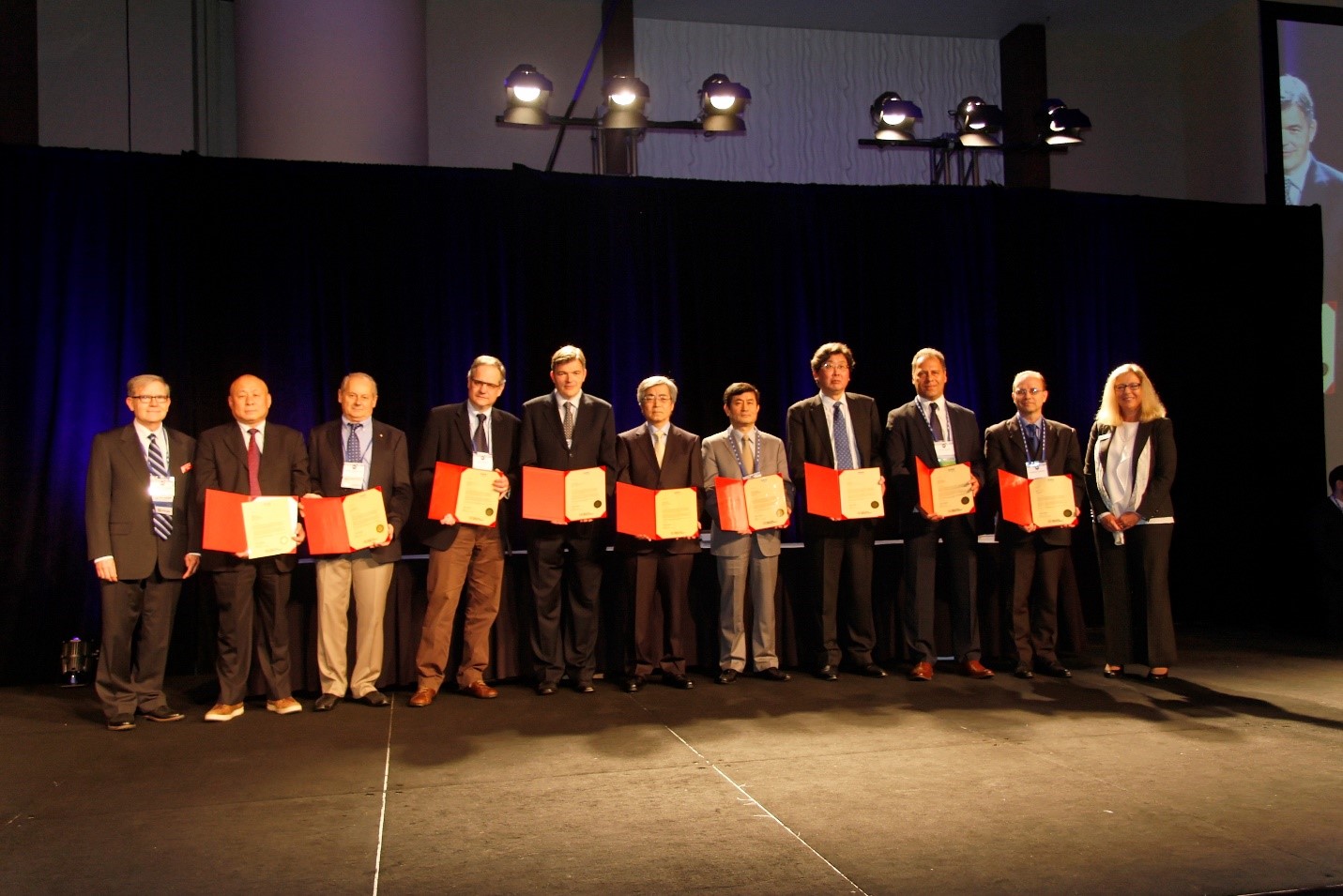
 The MOS-AK Compact Modeling Association, a global compact/SPICE modeling and Verilog-A standardization forum, held its 15th consecutive workshop as an integral engineering event at the ESSDERC/ESSCIRC on September 11, 2017 in Leuven (B). The event was coorganized by Jean-Michel Sallese, EPFL and Daniel Tomaszewski ITE (PL); its technical program was coordinated by Larry Nagel, OEC (USA) and Andrei Vladimirescu, UCB (USA); ISEP (FR) representing the International MOS-AK Board of R&D Advisers. Technical MOS-AK program promotion was provided by the Eurotraining and NEEDS of nanoHUB.org

A group of the international academic researchers and modeling engineers attended 13 technical compact modeling presentations covering full development chain form the nanoscaled technologies thru semiconductor devices modeling to advanced IC design support. The MOS-AK speakers have shared their latest perspectives on compact/SPICE modeling and Verilog-A standardization in the dynamically evolving semiconductor industry and academic R&D. The event featured advanced technical presentations covering compact model development, implementation, deployment and standardization covering full engineering R&D chain: TCAD/processing, device modeling, transistor level IC design support. These contributions were delivered by leading academic and industrial experts [1-12]. The presentations are available online for download at <http://www.mos-ak.org/leuven_2017/>. Selected best presentation will be recommended for further publication in the IJHSES.

The ESSDERC Track4 Devices and Circuit Compact Modeling has followed the MOS-AK workshop. The Track4 has been organized for very first time to highlight importance of the international compact/SPICE modeling R&D and foster its Verilog-A standardization. The ESSDERC Conference participants have attended four subsequent modeling sessions: Cross-Domain Compact Modeling [13-15]; Parameter Extraction [16-19]; Modeling of Emerging Devices [20-23]; Traps and Noise [24-28]. All the conference papers are available at IEEE Xplore and selected best papers will be recommended for further publication in J-EDS.

The MOS-AK Modeling Working Group has various deliverable and initiatives including a book entitled "Open Source TCAD/EDA Tools for Compact Modeling" and an open Verilog-A directory with models and supporting CAD/EDA software. The MOS-AK Association plans to continue its standardization efforts by organizing additional compact modeling meetings, workshops and courses in Europe, USA, India and China throughout 2017/2018 including:
  • 10th International MOS-AK Workshop in Silicon Valley (US) Dec. 2017
  • Spring MOS-AK Workshop in Strasbourg (F) March 2018
  • 3rd Sino MOS-AK Workshop in Beijing (CN) June, 2018
  • 16th MOS-AK ESSDERC/ESSCIRC Workshop in Dresden (D) Sept, 2018
About MOS-AK Association:
MOS-AK, an international compact modeling association primarily focused in Europe, to enable international compact modeling R&D exchange in the North/Latin Americas, EMEA and Asia/Pacific Regions. The MOS-AK Modeling Working Group plays a central role in developing a common language among foundries, CAD vendors, IC designers and model developers by contributing and promoting different elements of compact/SPICE modeling and its Verilog-A standardization and related CAD/EDA tools for the compact models development, validation/implementation and distribution. For more information please visit: mos-ak.org

REFERENCES:

MOS-AK/Leuven 2017 Workshop; Sept. 11, 2017
[1] ASCENT: Access to Leading European Nanoelectronics Technology
Jim Greer Tyndall (IRL)
[2] Junctionless Nanowire Transistors Performance: Static and Dynamic Modeling
Marcelo Antonio Pavanello Centro Universitario FEI (BR)
[3] Modeling and Analysis of Full-Chip Parasitic Substrate Currents
Renaud Gillon and Wim Schoenmaker ONSEMI (B), MAGWEL (B)
[4] Small- and large-signal RF modeling of silicon-based substrates
Martin Rack and Jean-Pierre Raskin Université catholique de Louvain (B)
[5] Tunnel FET C-V modeling: Impact of TFET C-V characteristics on inverter circuit performance
Chika Tanaka, Tetsufumi Tanamoto, and Masato Koyama, Toshiba (J)
[6] ASCENT Open Access to 14nm PDKs
T. Chiarella, N. Cordero, O. Faynot, Tyndall (IRL)
[7] Modelling of Surface Traps Effect on Semiconductor Nanowires
Ashkhen Yesayan*, Stepan Petrosyan*, Jean-Michel Sallese** *IRa, Armenia, **EPFL (CH)
[8] Measurement and modelling of specific behaviors in 28nm FD SOI UTBB MOSFETs of importance for analog / RF amplifiers
D. Flandre, V. Kilchytska, B. Kazemi, C. Gimeno and J.-P. Raskin UC Louvain
[9] IEEE EDS Compact Model Standardization
Benjamin Iniguez URV (SP)
[10] Is it possible to reduce the PDK development cost when demand for data is continuously increasing?
Andrej Rumiantsev MPI Corporation
[11] Optimal measurement parameters for accurate time-domain and spectral analyses of RTN
Léopold Van Brandt*, Valeriya Kilchytska*, Jean-Pierre Raskin*, Bertrand Parvais** and Denis Flandre*  *ELEN department, ICTEAM Institute, Université catholique de Louvain **imec
[12] Compact modeling for CMOS technology development and IC design
Daniel Tomaszewski ITE Warszaw (PL)

ESSDERC Trac4: Compact Modeling; Tuesday September 12, 2017 (11:00-12:20)
Cross-Domain Compact Modeling 
Chair: Wladek Grabinski - MOS-AK; Cristell Maneux – LIMS;
[13] INVITED: SPICE Modeling in Verilog-a: Successes and Challenges
Colin McAndrew
[14] SPICE Modeling of Light Induced Current in Silicon with 'generalized' Lumped Devices
Chiara Rossi, Pietro Buccella, Camillo Stefanucci, Jean-Michel Sallese
[15] Total Ionizing Dose Effects on Analog Performance of 28 nm Bulk MOSFETs
Chun-Min Zhang, Farzan Jazaeri, Alessandro Pezzotta, Claudio Bruschini, Gulio Borghello, Serena Mattiazzo

ESSDERC Trac4: Compact Modeling; Tuesday September 12, 2017 (14:00-15:20)
Parameter Extraction 
Chair: Thierry Poiroux - CEA; Marco Bellini – ABB;
[16] Nanometer CMOS Characterization and Compact Modeling at Deep-Cryogenic Temperatures
Rosario Marco Incandela, Lin Song, Harald Homulle, Fabio Sebastiano, Edoardo Charbon, Andrei Vladimirescu
[17] Cryogenic Characterization of 28 nm Bulk CMOS Technology for Quantum Computing
Arnout Beckers, Farzan Jazaeri, Andrea Ruffino, Claudio Bruschini, Andrea Baschirotto, Christian Enz
[18] A New Method for Junctionless Transistors Parameters Extraction
Renan Trevisoli, Rodrigo Doria, Michelly de Souza, Sylvain Barraud, Marcelo Pavanello
[19] Avalanche Compact Model Featuring SiGe HBTs Characteristics Up to BVCBO
Mathieu Jaoul, Didier Céli, Cristell Maneux, Michael Schröter, Andreas Pawlak

ESSDERC Trac4: Compact Modeling; Tuesday September 12, 2017 (16:40-18:00)
Modeling of Emerging Devices 
Chair: Jean-Michel Sallese - EPFL; Daniel Tomaszewski - ITE;
[20] Equivalent Circuit Model for the Electron Transport in 2D Resistive Switching Material Systems
Enrique Miranda, Chengbin Pan, Marco Villena, Na Xiao, Jordi Suñe, Mario Lanza
[21] Analytical Drain Current Model for Schottky-Barrier CNTFETs
Igor Bejenari, Michael Schroter, Martin Claus
[22] A General Circuit Model for Spintronic Devices Under Electric and Magnetic Fields
Meshal Alawein, Hossein Fariborzi
[23] Compact Physical Model of a-IGZO TFTs for Circuit Simulation
Matteo Ghittorelli, Fabrizio Torricelli, Carmine Garripoli, Jan-Laurens van der Steen, Gerwin Gelinck, Sahel Abdinia

ESSDERC Trac4: Compact Modeling; Wednesday September 13, 2017 (14:20-15:40)
Traps and Noise 
Chair: Benjamin Iniguez - URV; Sadayuki Yoshitomi - Toshiba;
[24] Modeling of Dynamic Trap Density Increase for Aging Simulation of Any MOSFET Circuits Mitiko Miura-Mattausch, Hidenori Miyamoto, Hideyuki Kikuchihara, Dondee Navarro, Tapas K. Maiti, Nezam Rohbani
[25] Comprehensive Compact Electro-Thermal GaN HEMT Model
Muhammad Alshahed, Mina Dakran, Lars Heuken, Mohammed Alomari, Joachim Burghartz
[27] Trap-Assisted Carrier Transport Through the Multi-Stack Gate Dielectrics of HKMG nMOS Transistors: a Compact Model
Apoorva Ojha, Nihar Ranjan Mohapatra
[28] A New Verilog-a Compact Model of Random Telegraph Noise in Oxide-Based RRAM for Advanced Circuit Design
Francesco Maria Puglisi, Nicolò Zagni, Luca Larcher, Paolo Pavan

--
You received this message because you are subscribed to the Google Groups "mos-ak" group.
To unsubscribe from this group and stop receiving emails from it, send an email to mos-ak+unsubscribe@googlegroups.com.
To post to this group, send email to mos-ak@googlegroups.com.
Visit this group at https://groups.google.com/group/mos-ak.
For more options, visit https://groups.google.com/d/optout.

Sep 19, 2017

A Large-Signal Monolayer Graphene Field-Effect Transistor Compact #Model for RF-Circuit Applications https://t.co/zoPkw74IK2


from Twitter https://twitter.com/wladek60

September 19, 2017 at 03:55PM
via IFTTT

Conduction Mechanisms in Metal-Base Vertical Organic Transistors by DC and LF-Noise Measurements https://t.co/ZSiOLFMquC #paper


from Twitter https://twitter.com/wladek60

September 19, 2017 at 03:07PM
via IFTTT

#Modeling of #Electromechanical Sensors & Systems https://t.co/K40OGzRV4U https://t.co/rdih9lNeei https://t.co/748KTEgqk7


from Twitter https://twitter.com/wladek60

September 19, 2017 at 12:08PM
via IFTTT

#Modeling of #Electromechanical Sensors & Systems https://t.co/K40OGzRV4U https://t.co/rdih9lNeei


from Twitter https://twitter.com/wladek60

September 19, 2017 at 12:08PM
via IFTTT

Sep 18, 2017

[paper] Design techniques for low-voltage analog integrated circuits

Matej Rakus, Viera Stopjakova, Daniel Arbet
Institute of Electronics and Photonics, Faculty of Electrical Engineering
and Information Technology Slovak University of Technology in Bratislava, Slovakia,
Journal of ELECTRICAL ENGINEERING, Vol.68 (2017), No.4, 245–255
DOI: 10.1515/jee-2017–0036

ABSTRACT: In this paper, a review and analysis of different design techniques for (ultra) low-voltage integrated circuits (IC) are performed. This analysis shows that the most suitable design methods for low-voltage analog IC design in a standard CMOS process include techniques using bulk-driven MOS transistors, dynamic threshold MOS transistors and MOS transistors operating in weak or moderate inversion regions. The main advantage of such techniques is that there is no need for any modification of standard CMOS structure or process. Basic circuit building blocks like differential amplifiers or current mirrors designed using these approaches are able to operate with the power supply voltage of 600 mV (or even lower), which is the key feature towards integrated systems for modern portable applications.
Fig: Parameter gm/ID versus the normalized drain current. MOS transistor operates in weak inversion (WI) for ic < 0.1. Strong inversion (SI) is for ic < 10. Everything in between belongs to the moderate inversion (MI) with center in ic = 1 

Sep 15, 2017

[paper] Principles and Trends in Quantum Nano-Electronics and Nano-Magnetics for Beyond-CMOS Computing

Ian A. Young and Dmitri E. Nikonov 
Components Research, Technology & Manufacturing Group
Intel Corp., Hillsboro, Oregon, USA
ESSDERC/ESSCIRC Leuven Sept.12-14, 2017

Abstract: An analysis of research in quantum nanoelectronics and nanomagnetics for beyond CMOS devices is presented. Some device proposals and demonstrations are reviewed. Based on that, trends in this field are identified. Principles for development of competitive computing technologies are formulated. Results of beyond-CMOS circuit benchmarking are reviewed.

TABLE I: Voltage Limitations For Computation Variables

Principle 1: Beyond-CMOS circuits require CMOS as an integral part. They will work alongside and augment CMOS computing blocks.

Principle 2: Some devices utilize collective states; this confers advantages of non-volatility or more energy efficient operation.

Principle 3: The choice for an optimal beyond-CMOS device will be determined by compatibility with an efficient and effective interconnect.

Principle 4: Low voltage devices – most direct way to low energy operation.

Principle 5: Start benchmarking with bottom up modeling of devices, build up from simple to more complicated circuits.

Principle 6: Majority gates (if easily implemented in a certain technology) enable more efficient circuits, especially for more complex computation functions.

Principle 7: Use electrical interconnects for longer propagation spans.

Principle 8: To convince the wider community, a non- volatile computing paradigm needs to be general enough to prove that it is valid for more than one architecture; while it needs to be specific enough to dispel claims that an essential aspect is missed.

Principle 9: Neuromorphic computing can be done more efficiently with beyond-CMOS circuits.

Conclusions: In summary, we have presented our view on the recent trends in quantum nanoelectronics and nanomagnetics for beyond CMOS devices, and outlined a few principles to make them realize practical computing technologies. We can pose a question for ourselves: What are the most promising directions of research? Where to double down on the effort? Among many equally important thrusts, our subjective preference is for magnetoelectric switching and neuromorphic beyond-CMOS circuits.