Mar 8, 2021

[paper] Open-Source Non-Contact Thermometer

Mohannad Jabbar Mnatia, Raad Farhood Chisabb, Azhar M.Al-Rawic, Adnan Hussein Alia 
and AlexVan den Bossched
An Open-Source Non-Contact Thermometer Using Low-Cost Electronic Components 
HardwareX (Elsevier) Available online 6 March 2021, e00183 
DOI: 10.1016/j.ohx.2021.e00183

aInstitute of Technology Baghdad, Middle Technical University, Baghdad, Iraq
bTechnical Institute Kut, Middle Technical University (MTU), Baghdad, Iraq
cElectrical Power Techniques Department, Al-Mamon University College, Baghdad, Iraq
dDepartment of Electrical Energy, Metals, Mechanical Constructions and Systems Ghent University, Ghent, Belgium

Abstract: Due to the spread of COVID-19 across the world and the increased need for non-contact thermometers to prevent the spread of disease, a new electronic thermometer has been designed and implemented for measuring human body temperature from a distance. This device is currently in use at building entrances to measure the body temperatures of employees, students, and customers. This system is designed using low-cost easy-to-assemble open-source electronic components. The system consists of seven main parts: an Arduino UNO microcontroller, an infrared (IR) thermometer for non-contact temperature measurements (GY-906 MLX90614ESF module), an IR motion sensor (TCRT 5000) for the purpose of contactless initiation of the system, a graphic LCD to display results, a DS3231 clock module for a real-time clock and calendar, and a micro-SD storage board to store device audio instructions.

Fig. The Operating Instructions Flowchart

Acknowledgements: This research did not receive any specific grant from funding agencies in the public, commercial, or not-for-profit sectors.


HardwareX - to promote free and open source design


from Twitter https://twitter.com/wladek60

March 08, 2021 at 09:53AM
via IFTTT

The Silicon Saxony industry association requests #European #semi industry funding


from Twitter https://twitter.com/wladek60

March 07, 2021 at 11:34PM
via IFTTT

Mar 7, 2021

[C4P] SISPAD 2021, September 27-29

International Conference on Simulation of Semiconductor Processes and Devices
SISPAD 2021, September 27-29
The abstract submission deadline April 9th.

Two-page abstract (text and figures, A4, 10 – 12 pt, pdf) should be sent to <sispad2021@utdallas.edu>  Authors of accepted papers are requested to submit a four-page final paper which will be published in the conference proceedings. The deadline for submission of the four-page final paper is July 9, 2021.

The SISPAD conference series provides an open forum for the presentation of the latest results and trends in process and device simulation. The conference is the leading forum for Technology Computer-Aided Design (TCAD) and is held alternatingly in the United States, Japan, and Europe in September.

Original contributions are solicited for SISPAD 2021 on topics that include but are not limited to:
  • Modeling and simulation of established semiconductor device, including FinFETs, GAA FETs, ultra-thin SOI devices, optoelectronic devices, TFTs, sensors, power electronic devices, and organic electronic devices.
  • Modeling and simulation of emerging devices including tunnel FETs, SETs, spintronic devices, straintronic devices, bio-electronic devices, and new material-based devices for various applications
  • Modeling and simulation of interconnects, including noise and parasitic effects
  • Modeling and simulation of all sorts of semiconductor processes, including first principles material design, and growth simulation of nano-scale fabrication
  • Advances in fundamental aspects of device modeling and simulation, including of charge, spin, and thermal transport, of collective states including spin/magnetic and charge, and of fluctuation, noise, and reliability.
  • Numerical methods and algorithms, including grid generation, user-interface, and visualization
  • Compact modeling for circuit simulation, including low-power, high frequency, and power electronics applications
  • Process/device/circuit co-simulation in context with system design and verification, including for emerging devices
  • Modeling and simulation of equipment, topography, lithography
  • Benchmarking, calibration, and verification of simulators

Mar 6, 2021

Virtual Si Museum /2109/ Oric1

Released on 5 March 1981, the ZX81 was the successor to 1980s ZX80 and, like its predecessor, was based around a Z80 CPU. Two years later, in summer 1983, I bought my Oric1, my first home computer based around a 8-bit 6502A running at amazing CPU clock of 1 MHz. For a reference, next to the Oric1 logo, is Raspberry Pi Zero based around a 32-bit ARM11 running at CPU clock of 1 GHz. What an astonishing CPU clock rate gain over less than 4decades = 1000 time faster:

Fig.1: The Oric1 and, next to its logo, Raspberry Pi Zero

Fig.2: The Oric1 connectivity (Left to right): display output to drive a PAL UHF TV;  RGB output on a 5 pin DIN 41524 socket; cassette recorder connector via a 7 Pin DIN 45329 socket; printer port, compatible with the then-standard Centronics parallel interface; expansion port allowing full access to the CPU's data address and control lines including external ROM and RAM access/expansion.
REF:
  • ZX81: https://en.wikipedia.org/wiki/ZX81
  • Oric1: https://en.wikipedia.org/wiki/Oric
  • MOS Technology 6502: https://en.wikipedia.org/wiki/MOS_Technology_6502
  • Centronics: https://en.wikipedia.org/wiki/Centronics
  • Raspberry Pi Zero: https://en.wikipedia.org/wiki/Raspberry_Pi#Pi_Zero


Mar 5, 2021

Released on 5 March 1981, the #ZX81 was the successor to 1980s #ZX80 and, like its predecessor, was based around a #Z80 #CPU https://t.co/lYSFzmr6FM #semi https://t.co/ZhgOZEIKls


from Twitter https://twitter.com/wladek60

March 05, 2021 at 04:52PM
via IFTTT

[i-Micronews] #Apple iPhone 12 series #mmWave #5G Chipset and Antenna - https://t.co/2mH1i77Se9 #semi https://t.co/BV10LY9Aqb


from Twitter https://twitter.com/wladek60

March 05, 2021 at 02:06PM
via IFTTT

[C4P] IEEE-NANO 2021 (Virtual) Montreal, Canada

IEEE-NANO 2021
Nanotechnology Flagship Conference
July 28-30, 2021 | Virtual from Montreal, Canada
Abstract Submission Deadline Extended: March 15, 2021 

CALL for PAPERS (download PDF)
Nanotechnology researchers will gather to exchange information across disciplines at the 21st IEEE International Conference in Nanotechnology, the flagship conference of the IEEE Nanotechnology Council. We hope you will join us at IEEE-NANO 2021, to be held virtually July 28th–30th, 2021 from Montreal. The IEEE-NANO 2021 is now calling for abstract submission. View Technical Interests Here and access the Submission System Here

We are delighted to share with you our confirmed distinguished plenary speakers:
  • John Polanyi, Nobel Laureate (University of Toronto)
  • Yury Gogotsi (Drexel University)
  • Luisa De Cola (University of Strasbourg)
  • Shelley Minteer (University of Utah)
Following the tradition of the NANO conferences, participants have the opportunity to publish their research in IEEE Xplore® and IEEE Transactions in Nanotechnology.
Important Dates:

Abstract Submission: March 15, 2021
Notice of acceptance: March 31, 2021
Submission of full paper for proceedings: May 1, 2021
Short notice proceedings for exceptional findings: June 1, 2021
Notification of short notice proceedings acceptance-revision-rejection: June 15, 2021

Mar 4, 2021

ICECCE-2021 Kuala Lumpur, Malaysia 12-13 June, 2021

3rd International Conference on
Electrical, Communication and Computer Engineering
ICECCE-2021
Kuala Lumpur, Malaysia
12-13 June, 2021

Dear authors,
Due to the requests of community, the deadline for paper submission has been extended to 31st March 2021 (his is firm date). You can present your papers online or physically.

We cordially invite you to attend and submit your papers for the IEEE - 3rd International Conference on Electrical, Communication, and Computer Engineering (ICECCE 2021), which will take place at Kuala Lumpur, Malaysia on 12-13 June 2021. The event will be highly international with the technical collaboration of Multimedia University Malaysia, Aksaray University, Turkey, University of Buner, Pakistan, International Islamic University Islamabad, Pakistan, and IEEE .

ICECCE 2021 aims to bring together leading academic and industrial researchers, scientists, engineers and practitioners to exchange the latest research ideas, methods, results, and share experiences, on all theoretical, experimental and applied aspects of Electrical, Communication and Computer Engineering. ICECCE 2021 will provide a unique interdisciplinary and multidisciplinary forum for researchers, practitioners and educators to present and discuss the most recent innovations, trends, practical challenges encountered and intelligent solutions adopted in their respective fields

The conference covers many topics under areas of Electrical, Communication and Computer Engineering and can be seen at www.icecce.com

ICECCE 2019 and ICECCE 2020 were technically co-sponsored and indexed by IEEE. The Proceedings of these conferences have been published at IEEE Xplore Digital Library. ICECCE 2019 and ICECCE 2020 are also indexed in SCOPUS. “Accepted papers will be submitted for inclusion into IEEE Xplore subject to meeting IEEE Xplore’s scope and quality requirements”

We shall be looking forward to your paper contributions and participation. We hope that attending the conference will provide an opportunity to meet academic and industry experts to exchange ideas about the latest technologies. We are sure that your stay in the beautiful and historic city of Kuala Lumpur will be very pleasant and enjoyable.

Important Dates:

  • Paper Due : 31 March, 2021
  • Acceptance Notification : 30 April, 2021
  • Camera Ready Due : 10 May, 2021
  • Conference Dates: 12 -13 June 2021

-- Regards -- ICECCE 2021 Conference Organizing Team;

Folllow us:  
Contact:
Dr. Athar Waseem; Conference Executive Chair
E-mail: 
athar.waseem@iiu.edu.pk
Phone: +92 334 8677790

Dr. Yunus UZUN; Conference Technical Chair
E-mail: yunusuzun38@hotmail.com
Phone: +90 532 6425237

#Chiplets For The Masses


from Twitter https://twitter.com/wladek60

March 03, 2021 at 11:37PM
via IFTTT

Mar 3, 2021

#GlobalFoundries (a unit of Abu Dhabi’s state-owned fund Mubadala)


from Twitter https://twitter.com/wladek60

March 03, 2021 at 06:38PM
via IFTTT

Mar 2, 2021

[paper] Predictive Hot-Carrier Aging Compact Model

Y. Xiang1,2, S. Tyaginov1,3,4, M. Vandemaele1,2, Z. Wu1,2, J. Franco1, E. Bury1, B. Truijen1, B.Parvais1,5, D. Linten1, B. Kaczer1
A BSIM-Based Predictive Hot-Carrier Aging Compact Model 
4A.4; IRPS March 21- 24 2021 

1imec, Leuven (B)
2Department of Electrical Engineering (ESAT), KU Leuven, Leuven (B)
3Institute for Microelectronics (IuE), TU Wien, Vienna (A)
4Ioffe Physical-Technical Institute of the Russian Academy of Sciences, Saint Petersburg (RU) 
5Department of Electronics and Informatics (ETRO/VUB), Brussels
 (B)

Abstract: The continued challenge of front-end-of-line transistor reliability has long demanded physics-based SPICE compact models, not only for service lifetime estimation, but also for agingaware device pathfinding with technology scaling and innovation. Here, we present a predictive hot-carrier-degradation (HCD) compact model built upon the industry-standard BSIM model, that conveniently embeds the essential HCD physics within common SPICE simulation flows. We leverage and augment the established, scalable electrostatics and transport in BSIM as the input to an analytical HCD interface states generation formalism, the result of which is in turn injected back into BSIM for a selfconsistent estimation of the threshold voltage (VTH) shift and the mobility degradation. Our approach readily exhibits fundamental, non-empirical predictabilities of the stress timeand the sensing bias- dependency of transistor-level degradation, without having to resort to a priori assumptions. This will further accommodate the irregular, arbitrary voltage waveforms in transient circuit operations, thus enabling efficient evaluation of the power-performance degradation at circuit level. The model ultimately aims to lay the groundwork for a reliability-aware design-technology co-optimization in device pathfinding. 
Fig: Schematic of the Pao-Sah DD current integral method used in commercial CMs [a-e] and the extrapolated piecewise Vch(y) by augmenting the BSIM model. In the Pao-Sah DD formalism, the actual Ids is calculated by the difference of the integral Ξ at the source (channel potential Vch=0) and at the “drift-diffusion limit” (at LDD, where channel potential Vch=VDS,eff), with the latter defined by velocity saturation or pinch-off. The Vch(y) is extrapolated by using the implicit assumptions in BSIM-BULK: the quadratic profile under gradual channel approximation (GCA) and the hyperbolic profile under the drain-side field assumption used in substratecurrent body-effect (SCBE). 

References:
[a] C. K. Dabhi. (2017). BSIM4 4.8.1 MOSFET Model: User’s Manual. [Online]. Available: https://bsim.berkeley.edu/models/bsim4/.
[b] H. Agarwal. (2017). BSIM-BULK106.2.0 MOSFET Compact Model: Technical Manual. [Online]. Available: https://bsim.berkeley.edu/models/bsimbulk/. 
[c] S. Khandelwal. (2015). BSIM-CMG 110.0.0 Multi-Gate MOSFET Compact Model: Technical Manual. [Online]. Available: https://bsim.berkeley.edu/models/bsimcmg/. 
[d] P. Kushwaha. (2017). BSIM-IMG 102.9.1 Independent Multi-Gate MOSFET Compact Model: Technical Manual. [Online]. Available: https://bsim.berkeley.edu/models/bsimimg/. 
[e] W. Grabinski et al., (2019) "FOSS EKV2.6 Verilog-A Compact MOSFET Model," ESSDERC 2019 - 49th European Solid-State Device Research Conference (ESSDERC), Cracow, Poland, 2019, pp. 190-193, doi: 10.1109/ESSDERC.2019.8901822
[Online] Available: https://github.com/ekv26/model


[The Register] Wuhan Hongxin #semi 7nm ambitions are dust. One of #China’s next-generation #chipmakers appears to have collapsed, potentially hampering the nation’s march to silicon-self-sufficiency https://t.co/Vx2bi2TUeq https://t.co/1iCKL4KcJu


from Twitter https://twitter.com/wladek60

March 02, 2021 at 10:49AM
via IFTTT

Mar 1, 2021

Pumping perovskites into a #semi platform https://t.co/DC9C7OL1q8 https://t.co/gle4f9tNrB


from Twitter https://twitter.com/wladek60

March 01, 2021 at 03:44PM
via IFTTT

[papers] compact/SPICE modeling

[1] M. Müller, P. Dollfus and M. Schröter, "1-D Drift-Diffusion Simulation of Two-Valley Semiconductors and Devices," in IEEE Transactions on Electron Devices, vol. 68, no. 3, pp. 1221-1227, March 2021, doi: 10.1109/TED.2021.3051552.

Abstract: A two-valley formulation of 1-D drift-diffusion transport is presented that takes the coupling between the valleys into account via a new approximation for the nonlocal electric field. The proposed formulation is suitable for the simulation of III–V heterojunction bipolar transistors as opposed to formulations that employ the single electron gas approximation with a modified velocity-field model, which also causes convergence problems. Based on Boltzmann transport equation simulations, model parameters of the proposed two-valley formulation are given for GaAs, InP, InAs, and GaSb at room temperature. Applications of the new formulation are also demonstrated. 
Code/Dataset: This article contains datasets made available via IEEE DataPort, a repository of datasets intended to facilitate analysis and enable reproducible research. Click the dataset name below to access it on the IEEE DataPort website.

[2] A. Rawat et al., "Experimental Validation of Process-Induced Variability Aware SPICE Simulation Platform for Sub-20 nm FinFET Technologies," in IEEE Transactions on Electron Devices, vol. 68, no. 3, pp. 976-980, March 2021, doi: 10.1109/TED.2021.3053185.

Abstract:We propose an experimentally validated physics-based process-induced variability (PIV) aware SPICE simulation framework–enabling the estimation of performance variation due to line-edge-roughness (LER), metal-gate-granularity (MGG), random-dopant-fluctuation (RDF), and oxide-thickness-variation (OTV) at sub-20 nm technology node devices. The framework utilizes LER, RDF, OTV, and MGG defining parameters such as fin-edge correlation coefficient (ρ), autocorrelation length (Λ), grain-size (GS), σ[EOT], etc. as the inputs, and produces IdVg distribution of ensemble size 250 as an output. We have validated the framework against 14 nm FinFET experimental data for IdVg trends as well as for the threshold-voltage (Vth), ON-current (Ion), and subthreshold slope (SS) distributions for a range of device dimensions with a reasonably good match. The worst and the best case R square errors are 0.64 and 0.98, respectively, for the validation. The very nature of the proposed framework allows the designers to use it for a vast range of process technologies. Such models are of dual importance, as it enables a PIV aware prediction of circuit-level performance, and provides a platform to estimate PIV parameters efficiently, on-par with sophisticated structural characterization tools.

[3] Blake W. Nelson, Andrew N. Lemmon, Sergio J. Jimenez, H. Alan Mantooth, Brian T. DeBoi, Christopher D. New, Md Maksudul Hossain, "Computational Efficiency Analysis of SiC MOSFET Models in SPICE: Dynamic Behavior," in IEEE Open Journal of Power Electronics, vol. 2, pp. 106-123, 2021, doi: 10.1109/OJPEL.2021.3056075.

Abstract: Transient simulation of complex converter topologies is a challenging problem, especially in detailed analysis tools like SPICE. Transistor models presented for SPICE are often evaluated by accuracy, with less consideration for the computational cost of model elements. In order to optimize models for application simulations, this research quantifies the relative simulation performance of modeling approaches and contextualizes the results with regard to accuracy. It is well established that the primary contributor to semiconductor dynamic behavior is the voltage-dependent interelectrode capacitances. Therefore, this study isolates these model components to resolve their influence on model accuracy and run-time. Both the voltage-dependencies modeled, and the mathematic formulation chosen strongly influence the accuracy of interelectrode capacitance models. In addition to these factors, the specific implementation chosen within SPICE also determines simulation performance. Through careful evaluation of these factors, this study offers specific recommendations for optimal implementations of interelectrode capacitances in SPICE.
Fig: DPT system schematic, components, and metrology.

[4] Sherif M. Sharroush & Yasser S. Abdalla; Parameter extraction and modelling of the MOS transistor by an equivalent resistance, Mathematical and Computer Modelling of Dynamical Systems, (2021) 27:1, 50-86, DOI: 10.1080/13873954.2020.1857790

Abstract: During the analysis of multi-transistor circuits, the need arises to evaluate the time delay or the power consumption of the circuit. Due to the complexity of the transistor model, several complicated equations arise from which a compact-form solution cannot be obtained and a suitable physical insight cannot be drawn. With this regard, two contributions are presented in this paper. The first one is a fully analytical parameter extraction approach to be applied on the MOS transistors. The second one is a quantitative method for simplifying the analysis of MOS circuits by modelling the MOS transistor by a suitable equivalent resistance adopting the time-delay or the power-consumption equivalence criteria. The parameter-extraction method is verified by using the extracted parameters in the derived expressions according to the second contribution. Compared to other representations, the agreement of the proposed model with the simulation results is very good.
Fig: Finding Vthn0 as the intercept of the linear portion of the Id-Vgs characteristics with the horizontal axis. The curve corresponds to Vds=1V. The term ‘exact relationship’ means data from the simulation results


#SEMI Applauds President Biden, Bipartisan Congressional Leaders for Supporting #Semi Supply Chain Incentives


from Twitter https://twitter.com/wladek60

March 01, 2021 at 09:37AM
via IFTTT

Feb 28, 2021

ToM 2021

Topics on Microelectronics
ToM 2021

Each event typically consists of five long talks/lectures on different topics (of three hours each, a sufficient time to give both overview and advanced details about the topic), given by academic professors or qualified experts coming from companies or research centers. In this way the academic and industrial approaches for research and state-of-the art progress are presented.In the last years, an increasing number of microelectronic companies are establishing design centers in the Milan area (Allegro Microsystems, AMS, Bosch, Catena, Inphi, Huawei, Infineon Technologies, Maxim Integrated, Micron, SK-Hynix, TDK-Invensense, Photeon Technologies, Silicon Mitus, STMicroelectronics, etc….). In this scenario, an advanced educational activity is a key point for success. The ToM events are addressing researchers, designers from companies, and students (Master and Ph. D.), who want to improve their knowledge in the microelectronic field.

Different topics are addressed in each event. This is intentionally done in order to cover as much as possible the wide spectrum of challenges in the present microelectronic world.

The courses are organized together with the Italian Chapter of the IEEE Solid-State Circuit Society and the University of Milano-Bicocca.

ToM2021/1 and ToM2021/2 courses will be held online on May, 25th-27th, 2021 and September, 21st-23rd, 2021, respectively. Registration is mandatory to attend the courses. Registered participants will receive:

  • on-line attendance to all lectures
  • pdf material for all lectures
  • certificate of participation
  • final exam with certificate (if needed)

Organizing Committee

Scientific Director: Prof. Andrea Baschirotto (andrea.baschirotto@unimib.it)
Scientific Co-Director: Prof. Piero Malcovati (piero.malcovati@unipv.it)

Registration

Registration to the ToM Courses has to be performed using the general online registration form.
Payment can be performed via Credit Card or Paypal directly through the online system.
The registration includes the membership to InnoTechEvents for year 2021.

University of Milano-Bicocca people have to use the dedicated UniMIB online registration form.

Program

ToM2021/1 – May 25-27, 2021
Online, Lectures in English

25 May 2021

14:00 – 17:30 Pietro Andreani (Lund University, Sweden), “Integrated harmonic oscillators”

26 May 2021

09:00 – 12:30 Dante Muratore (TU Delft, The Netherlands), “Circuit challenges in implantable brain-machine interfaces”

14:00 – 17:30 Bernhard Wicht (Leibniz University Hannover, Germany), “Analog building blocks of DC-DC converters”

27 May 2021

09.00 – 12:30 Tristan Meunier (CNRS, France), “Quantum computing with CMOS technology”

14:00 – 17:30 Gabriele Manganaro (Mediatek, USA), “High-speed digital-to-analog converters”

ToM2021/2 – September 21-23, 2021
Online, Lectures in English

21 September 2021

14:00 – 17:30 Jussi Jansson (Oulu University, Finland) - “Time-to-digital converters and related applications”

22 September 2021

09:00 – 12:30 Luca Scandola (Infineon Technologies, Italy), “Introduction to DC-DC conversion suitable for automotive application: from the theory to the modelization with practical examples”

14:00 – 17:30 Benoit Bakeroot (Ghent University, Belgium), “GaN semiconductor devices for power electronics: overview, status and future perspectives”

23 September 2021

09.00 – 12:30 Qiang Li (UETSC, China), “Subthreshold and near-threshold ADC techniques”

14:00 – 17:30 Andrea Mazzanti (University of Pavia, Italy) and Enrico Monaco (Inphi, Italy), “Introduction and advances in serial links”

John von #Neumann: From the #Manhattan Project to the #Princeton Architecture https://t.co/xU9zjC15C2 #semi https://t.co/aX4ApJr5Ch


from Twitter https://twitter.com/wladek60

February 28, 2021 at 05:34PM
via IFTTT

Feb 27, 2021

Feb 26, 2021

[DAY 2] 1st Asia/South Pacific MOS-AK Workshop

Arbeitskreis Modellierung von Systemen und Parameterextraktion
Modeling of Systems and Parameter Extraction Working Group
1st Asia/South Pacific MOS-AK Workshop
(virtual/online) FEB. 25-26, 2021

Day2: FEB.26
Session C Chair: Sadayuki Yoshitomi, Kioxia (J)

[8] eSim: An open source CAD software for circuit simulation
Kannan Moudgalya
IIT Bombay (IN)

[9] A modular approach to next generation Qucs
Felix Salfelder and Mike Brinson
QUCS Team; Centre for Communications Technology, London Metropolitan University (UK)

[12] Machine learning-based approach to model and analyze GaN power devices
Tian-Li Wu
National Yang Ming Chiao Tung University, Taiwan (TW)

[11] TCAD-inspired compact modeling approach
Sung-Min Hong and Kwang-Woon Lee
Gwangju GIST (KR)

Session D Chair: Sheikh Aamir Ahsan, NIT Srinagar (IN)
[10] An Innovative Technique for Ultrafast Carrier Dynamics and THz Conductivities of Semiconductor Nanomaterials
Praveen Kr. Saxena and Fanish Kr. Gupta
Tech Next Lab, Lucknow (IN)

[13] Compact Modeling of 3D NAND Flash Memory for Diverse Unconventional Analog Applications
Shubham Sahay
IIT Kanpur (IN)

[14] Steep Subthreshold Slope PN-Body Tied SOI-FET for Ultralow Power LSI, Sensor, and Neuromorphic Chip
Takayuki Mori and Jiro Ida
Kanazawa Institute of Technology, Nonoichi (J)

[Pic] Group photo of selected MOS-AK participants attending 2nd Day of the workshop


[DAY 1] 1st Asia/South Pacific MOS-AK Workshop

Arbeitskreis Modellierung von Systemen und Parameterextraktion
Modeling of Systems and Parameter Extraction Working Group
1st Asia/South Pacific MOS-AK Workshop
(virtual/online) FEB. 25-26, 2021

DAY 1: FEB. 25, 2021
Session A Chair: Usha Gogineni, ams AG, Hyderabad (IN)

[1] New Insights in Low Frequency Noise Characteristics in PE-BJTs
Peijian Zhang and Ma Long
Science and Technology on Analog Integrated Circuit Laboratory; WHU (CN), Keysight Technologies (US)

[2] Direct white noise characterization of short-channel MOSFETs
K. Ohmori and S. Amakawa
DeviceLab, Tsukuba (J)

[3] SPICE Modeling of 2D-material based FETs with Schottky-barrier contacts
Sheikh Aamir Ahsan
Nanoelectronics Research and Development Group, NIT Srinagar, Jammu and Kashmir (IN)


[4] Physics-based model of SiC MOSFETs including high voltage and current regions
Sourabh Khandelwal, Cristino Salcines, and Ingmar Kallfass
Macquarie University Sydney (AU), University of Stuttgart (D)

Session B Chair: Daniel Tomaszewski, IMiF, Warszaw (PL)
[5] Compact Modeling for Gate-All-Around FET Technology
Avirup Dasgupta
IIT Roorkee (IN)


[6] BSIM-HV: Advanced High Voltage MOSFET Compact Model
Harshit Agarwal
IIT Jodhpur (IN)

[7] ASCENT+ Transnational Access for the nanoelectronics
Georgios Fagas
Tyndall (IE)

[Pic] Group photo of selected MOS-AK participants attending 1st Day of the workshop

[https://t.co/42ahdl8o1h] Study Captures #India's Rise in #Nanoelectronics Research https://t.co/xGqsmBiKKa #semi https://t.co/XNnB7RP3Fn


from Twitter https://twitter.com/wladek60

February 26, 2021 at 02:32PM
via IFTTT

President Biden signed an executive order Wednesday addressing growing concern over a global semiconductor shortage hampering the production of goods like automobiles and smartphones. https://t.co/JGZVSGVeSF #semi https://t.co/vWAg7EaYW8


from Twitter https://twitter.com/wladek60

February 26, 2021 at 02:16PM
via IFTTT

Feb 25, 2021

[Infineon Technologies] #quantum #computing development


from Twitter https://twitter.com/wladek60

February 24, 2021 at 11:46PM
via IFTTT

Feb 23, 2021

[papers] Compact/SPICE Modeling

[1] Wang, Jie; Chen, Zhanfei; You, Shuzhen; Bakeroot, Benoit; Liu, Jun; Decoutere, Stefaan; "Surface-Potential-Based Compact Modeling of p-GaN Gate HEMTs" Micromachines (2021) 12, no. 2: 199; https://doi.org/10.3390/mi12020199

Abstract: We propose a surface potential (SP)-based compact model of p-GaN gate high electron mobility transistors (HEMTs) which solves the Poisson equation. The model includes all possible charges in the GaN channel layer, including the unintended Mg doping density caused by out-diffusion. The SP equation and its analytical approximate solution provide a high degree of accuracy for the SP calculation, from which the closed-form I–V equations are derived. The proposed model uses physical parameters only and is implemented in Verilog-A code.

Fig: The equivalent circuit of the capacitance of field plates (FPs) of a p-GaN gate HEMT.


[2] Chen, H. and He, L.,  The spatial and energy distribution of oxide trap responsible for 1/f noise in 4H-SiC MOSFETs. Journal of Physics Communications, JPCO-101816.R1 (2021)

Abstract: Low-frequency noise is one of the important characteristics of 4H-SiC metal-oxide-semiconductor field-effect transistors (MOSFETs) that is susceptible to oxide traps. Drain-source voltage noise models of 4H-SiC MOSFETs under low–drain-voltage and inverse condition were proposed by considering the spatial and energy non-uniform distribution of the oxide trap, based on the McWhoter model for uniform trap distribution. This study performed noise experiments on commercial 4H-SiC MOSFETs, and revealed that the non-uniform spatial and non-uniform energy distribution caused new 1/f noise phenomenon, different from that under uniform spatial and energy distribution. By combining experimental data and theoretical models, the spatial and energy distribution of oxide traps of these samples were determined.
Fig: Adaptive circuit for 4H-SiC MOSFET noise measurement
in the frequency 1 Hz-10kHz ranged


Feb 22, 2021

[Kioxia] Less is more: the challenge of #3D-#NAND memory https://t.co/N5eEZAOL16 #semi https://t.co/Tm7fNXTynD


from Twitter https://twitter.com/wladek60

February 22, 2021 at 06:24PM
via IFTTT

#TSMC vs #Intel https://t.co/kNtoOcTRFx #semi @mannerisms @semiwiki https://t.co/eMLyKrFdY1


from Twitter https://twitter.com/wladek60

February 22, 2021 at 02:49PM
via IFTTT

[https://t.co/FrgrQhA6mP] #India needs chipset manufacturers — lots of them. Here is why. https://t.co/VrJw27rpFp #semi https://t.co/nq0KKtrJVP


from Twitter https://twitter.com/wladek60

February 22, 2021 at 02:07PM
via IFTTT

[3D Printing Industry] Researchers open up low-cost #opensource #microfluidics #3D printing - https://t.co/VwPoWIzI72 #semi https://t.co/OyfmccoCb9


from Twitter https://twitter.com/wladek60

February 22, 2021 at 02:04PM
via IFTTT

Feb 19, 2021

Virtual Si Museum /2107/ TG4 and TG50

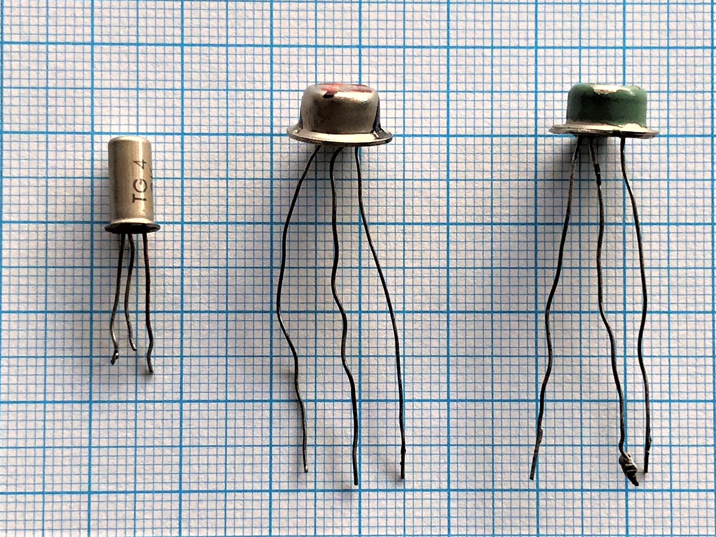
The TG1-TG5 series transistor are the first industrially mass-produced BJT transistors in Poland. The serial production was started by the TEWA Semiconductor Factory, Warsaw, in early1960s. Then, the TG50-TG55 series, was also manufactured by the TEWA in 1961–1962. 

The TG4 (see Pic: below) is low power, low frequency, pnp germanium (Ge) alloy transistor (with 75 mW max collector power) [1].

The TG50 (below) is medium power, low frequency,  pnp germanium (Ge) alloy transistor (with 175 mW max collector power) [2].

An initial stage of Polish semiconductor microelectronics research activities has been reviewed by Prof. Jerzy Pułtorak. In his paper [3], he has reviewed activities of leading Polish R&D groups starting from Department of Electronics, Polish Academy of Sciences (PAN) founded on July 4, 1952 till foundation of the Instytut Technologii Elektronowej (ITE, Warsaw) early 1960 (now Sieć Badawcza Łukasiewicz - Instytut Mikroelektroniki i Fotoniki).  The first, in Poland, experimental germanium point-contact transistor TP-1 [4] has been developed by Prof. Rosinski just after John Bardeen, Walter Brattain and William Shockley have invented a semi-conductor triode (transistor) [5] on December 23, 1947.

Pic: TG4 and two TG50 by the TEWA Semiconductor Factory, Warsaw (PL)

References: 
[1] TG1-5 / PL Wikipedia/ https://pl.wikipedia.org/wiki/TG1-5
[2] TG50-5  / PL Wikipedia/ https://pl.wikipedia.org/wiki/TG50-55
[3] J. Pułtorak, "60 years of polish transistors," 2014 Proceedings of the 21st International Conference Mixed Design of Integrated Circuits and Systems (MIXDES), Lublin, Poland, 2014, pp. 15-21, doi: 10.1109/MIXDES.2014.6872144.
[4] W.Rosinski, J.Groszkowski, “Doswiadczalne tranzystory punktowe model TP” (“Experimental point-cotact transistors model TP”), Arch. Elektrot. 4, 1955, p. 381
[5] J.Bardeen, H.W.Brattain, “The transistor, a semi-conductor triode”, Phys.Rev.74, 7, 1954, p.230


Feb 18, 2021

#Linux Foundation, #DARPA collaborate on #opensource for #5G https://t.co/AHyNjyTjHJ #semi https://t.co/2BrfkspWSl


from Twitter https://twitter.com/wladek60

February 18, 2021 at 09:02PM
via IFTTT

[mos-ak] [Final Program] 1st Asia/South Pacific MOS-AK Workshop (Online) FEB. 25-26, 2021


Together with IEEE Young Professionals (at iitk.ac.in), the MOS-AK workshop online host as well as all the Extended MOS-AK TPC Committee, we have the pleasure to invite to the very first Asia/South Pacific MOS-AK Workshop which will be Virtual/Online event. Scheduled, 1st Asia/South Pacific MOS-AK Workshop, aims to strengthen a network and discussion forum among experts in the field, enhance open platform for information exchange related to compact/SPICE modeling and Verilog-A standardization, bring people in the compact modeling field together, as well as obtain feedback from technology developers, circuit designers, and TCAD/EDA tool developers and vendors.

The MOS-AK workshop program is available online

Venue: Virtual/Online MOS-AK Workshop - FEB. 25-26, 2021
  • Day 1 (FEB.25) begins: 8:00 in Europe; 12:30 in India; 15:00 in China
  • Day 2 (FEB.26) begins: 8:00 in Europe; 12:30 in India;15:00 in China
Registered participant will receive online meeting invitation
(any related enquiries can be sent to register@mos-ak.org)

Postworkshop Publications: Selected best MOS-AK technical presentation will be recommended for further publication in a special Solid State Electronics (SSE) issue on compact modeling.

W.Grabinski on the behalf of International MOS-AK Committee
WG18022021

--
You received this message because you are subscribed to the Google Groups "mos-ak" group.
To unsubscribe from this group and stop receiving emails from it, send an email to mos-ak+unsubscribe@googlegroups.com.
To view this discussion on the web visit https://groups.google.com/d/msgid/mos-ak/CALp-Rj84YhCntEfry9%3DmQkeprAkB6cWtMcZ4RnFvVSNgh7pa7g%40mail.gmail.com.