Arbeitskreis Modellierung von Systemen und Parameterextraktion
Modeling of Systems and Parameter Extraction Working Group
1st Asia/South Pacific MOS-AK Workshop
(virtual/online) FEB. 25-26, 2021
Day2: FEB.26
Session C Chair: Sadayuki Yoshitomi, Kioxia (J)
[8] eSim: An open source CAD software for circuit simulation
Kannan Moudgalya
IIT Bombay (IN)

[9] A modular approach to next generation Qucs
Felix Salfelder and Mike Brinson
QUCS Team; Centre for Communications Technology, London Metropolitan University (UK)

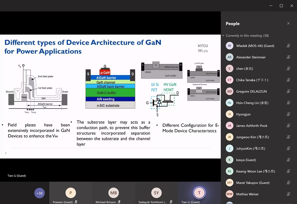
[12] Machine learning-based approach to model and analyze GaN power devices
Tian-Li Wu
National Yang Ming Chiao Tung University, Taiwan (TW)
Tian-Li Wu
National Yang Ming Chiao Tung University, Taiwan (TW)
[11] TCAD-inspired compact modeling approach
Sung-Min Hong and Kwang-Woon Lee
Gwangju GIST (KR)

Session D Chair: Sheikh Aamir Ahsan, NIT Srinagar (IN)
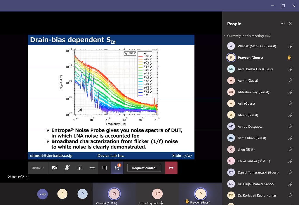
[10] An Innovative Technique for Ultrafast Carrier Dynamics and THz Conductivities of Semiconductor Nanomaterials
Praveen Kr. Saxena and Fanish Kr. Gupta
Tech Next Lab, Lucknow (IN)

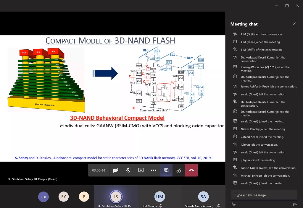
[13] Compact Modeling of 3D NAND Flash Memory for Diverse Unconventional Analog Applications
Shubham Sahay
IIT Kanpur (IN)
Shubham Sahay
IIT Kanpur (IN)
[14] Steep Subthreshold Slope PN-Body Tied SOI-FET for Ultralow Power LSI, Sensor, and Neuromorphic Chip
Takayuki Mori and Jiro Ida
Kanazawa Institute of Technology, Nonoichi (J)
Takayuki Mori and Jiro Ida
Kanazawa Institute of Technology, Nonoichi (J)

[Pic] Group photo of selected MOS-AK participants attending 2nd Day of the workshop