Jan 11, 2021

[paper] Neuromuscular Junction‐on‐a‐Chip

Rianne de Jongh1, Xandor M. Spijkers1,2, Svetlana Pasteuning‐Vuhman1
Paul Vulto2 R. Jeroen Pasterkamp1
Neuromuscular Junction‐on‐a‐Chip: 
ALS disease modeling and read‐out development in microfluidic devices
Journal of Neurochemistry 
Open Access 31 December 2020
DOI: 10.1111/jnc.15289 

1 Department of Translational Neuroscience, University Medical Center Utrecht Brain Center, Utrecht University, Utrecht, The Netherlands.
2 Mimetas B.V., Organ-on-a-chip Company, Leiden, The Netherlands

Abstract: Amyotrophic lateral sclerosis (ALS) is a fatal and progressive neurodegenerative disease affecting upper and lower motor neurons with no cure available. Clinical and animal studies reveal that the neuromuscular junction (NMJ), a synaptic connection between motor neurons and skeletal muscle fibers, is highly vulnerable in ALS and suggest that NMJ defects may occur at early stages of the disease. However, mechanistic insight into how NMJ dysfunction relates to the onset and progression of ALS is incomplete, which hampers therapy development. This is, in part, caused by a lack of robust in vitro models. The ability to combine microfluidic and induced pluripotent stem cell (iPSC) technologies has opened up new avenues for studying molecular and cellular ALS phenotypes in vitro. Microfluidic devices offer several advantages over traditional culture approaches when modeling the NMJ, such as the spatial separation of different cell types and increased control over the cellular microenvironment. Moreover, they are compatible with 3D cell culture, which enhances NMJ functionality and maturity. Here, we review how microfluidic technology is currently being employed to develop more reliable in vitro NMJ models. To validate and phenotype such models, various morphological and functional read‐outs have been developed. We describe and discuss the relevance of these read‐outs and specifically illustrate how these read‐outs have enhanced our understanding of NMJ pathology in ALS. Finally, we share our view on potential future directions and challenges.

FIG: Overview of some of the morphological and functional read-outs that can be used
in NMJ-on-a-chip models for studying ALS disease mechanisms. 

Acknowledgements: We thank Dr. Ewout Groen and Prof. Eran Perlson for carefully reading the manuscript, and Frederik Schavemaker for help with preparing the Figures. Work in the laboratory of R.J.P. is supported by the ALS Stichting Nederland (TOTALS, ALS-on-a-Chip) and by the MAXOMOD and INTEGRALS consortia under the frame of E-Rare-3, the ERANet for Research on Rare Diseases.

#Intel Talks With #TSMC, #Samsung to Outsource Some Chip #semi Production https://t.co/nMJIjXsben https://t.co/u8mpOgXf6R


from Twitter https://twitter.com/wladek60

January 11, 2021 at 10:10AM
via IFTTT

Jan 8, 2021

Low-power #MEMS #microphone https://t.co/A6tcnAt4km #semi https://t.co/CSEfyDEsgm


from Twitter https://twitter.com/wladek60

January 08, 2021 at 02:23PM
via IFTTT

[C4P] Spintronics-Devices and Circuits

Call for Papers for a Special Issue of 
IEEE Transactions on Electron Devices on
Spintronics-Devices and Circuits
Submission deadline: 30 September, 2021 
Publication date: April 2022

Spintronics is one of the emerging fields for the next-generation nanoscale devices offering better memory and processing capabilities with improved performance levels. It demonstrates great potential in the post-Moore era. Ever since the discovery of Giant Magneto-Resistance (GMR) effect in 1988, spintronics has shown rapid progress. Recent advances have expanded this technology to the entire electronics industry of sensors, memories, oscillators, quantum information processors, computer architecture, brain inspired computing and various other fields. Spintronics is now one of the most researched areas and is on the verge of becoming a mainstream technology. A hard disk drive (HDD) invented by IBM in 1956, now has a global market revenue of approximately $12bn. Other emerging field of application for this technology is magnetic field sensors that showcased a market revenue of ~$19b in 2018. The magnetic memory production at major foundries such as Samsung, Globalfoundries, Western Digital and TSMC marks the adoption of spintronics technology. However, in order to meet the ever-increasing demands of the industry, innovation in terms of modeling, design, materials, processes, circuits and applications are required. This Special Issue of the IEEE Transactions on Electron Devices will feature the most recent developments and the state-of-the-art in the field of spintronic devices, circuits and new architectures for high performance.

Topics of interest include, but are not limited to:
Materials:
Ferromagnets, Antiferromagnets, 2D material for better spin manipulation and spin logic devices, Heusler alloys, dilute magnetic semiconductors (DMS), half-metallic ferromagnet (HMF)
Transport mechanism:
Spin accumulation, injection and detection in spin devices, spin pumping techniques, angular momentum transportation by spin polarized currents, spin waves, magnons, spin hall effect, spin transfer torque, enhancement in spin diffusion length and coherence time
Spintronics devices:
STT-MRAM, SOT-MRAM, VCMA-MRAM, domain-wall, skyrmions, nano-oscillators, sensors etc. Low power and high-speed switching schemes for spintronic devices.
Optoelectronics and Spintronics:
All-optical switching of magnetization, inverse magnetooptical effects, single shot optical switching, modeling circuit and architecture level design for ultra-fast laser excitation
Memories:
High storage density MRAM, enhancement in power efficiency and speed
In-memory computing:
Spintronics based in-memory computing/ processing circuits/architectures and applications
Quantum Computing:
Quantum information processing, protocol for communication, computation and sensing, algorithms, spin qubit, systems and applications, spintronics-based quantum memories
Neuromorphic computing:
Hardware implementation of neural networks, analog and digital, architectures and applications
Fabrication:
Fabrication and characterization of novel materials and devices, hybrid spintronics integration and fabrication
Spintronics based circuits:
Reconfigurable and programmable spintronics based circuits, Security applications including RNG and PUF, ADC/DAC, reliability and power performance analysis of spintronics based devices and circuits

Submission instructions: Please visit the following link to download the templates:
http://www.ieee.org/publications_standards/publications/authors/author_templates.html
In your cover letter, please indicate that your submission is for this special issue.
Submission site: https://mc.manuscriptcentral.com/ted

The papers must present original material that has not been copyrighted, published or accepted
for publications in any other archival publications, that is not currently being considered for
publications elsewhere, and that will not be submitted elsewhere while under considerations
by the Transactions on Electron Devices.

Guest Editors:
1. Prof. Brajesh Kumar Kaushik, Department of Electronics and Communication Engineering, Indian Institute of Technology Roorkee, INDIA (Lead Guest Editor)
2. Dr. Sanjeev Aggarwal, Everspin Technologies Inc., USA
3. Prof. Supriyo Bandyopadhyay, Department of Electrical and Computer Engineering, VCU College of Engineering, USA
4. Prof. Debanjan Bhowmik, Department of Electrical Engineering, Indian Institute of Technology Delhi, INDIA
5. Dr. Vivek De, Circuits Research Lab, Intel, USA
6. Dr. Bernard Dieny, SPINTEC, IRIG/CEA Grenoble, FRANCE
7. Prof. Wang Kang, School of Microelectronics, Beihang University, CHINA
8. Prof. S.N. Piramanayagam, School of Physical & Mathematical Sciences - Division of Physics & Applied Physics, Nanyang Technological University, SINGAPORE
9. Prof. Kaushik Roy, School of Electrical and Computer Engineering, Purdue
University, USA
10. Prof. Ashwin A. Tulapukur, Department of Electrical Engineering, Indian Institute of Technology Bombay, INDIA

[C4P] New simulation methodologies for next-generation TCAD

Call for Papers for a Special Issue of
IEEE Transactions on Electron Devices on
"New simulation methodologies for next-generation TCAD" 
Submission deadline: February 28, 2021 
Publication date: November 2021

Technology Computer Aided Design is used to simulate semiconductor processes and devices,a field which has become increasingly complex and heterogeneous. Processing of integrated circuits requires nowadays over 400 process steps, and the resultant devices often have a complicated 3D structure and contain various materials. The full device behavior can only be understood by considering effects on all length scales from atomistic (interfaces, defects etc.) over nanometric (quantum confinement, non-bulk properties etc.) to full chip dimensions (strain, heat transport etc.), and time scales from femtoseconds to seconds. Voltages, currents and charges have been scaled to such low levels that electronic noise, statistical effects and process variations have a strong impact. Devices based on new materials (e.g. 2D crystals) and physical principles (ferroelectrics, magnetic materials, qubits etc.) challenge standard TCAD approaches. While the simulation methods developed by the physics community can describe the basic device behavior, they often lack important simulation capabilities like, for example, transient simulations or integration with other TCAD tools and are too slow for daily use. Due to the complexity of semiconductor technology, it becomes more and more difficult to assess the impact of a change in processing or device structure on circuit performance by looking at a single aspect of an isolated device under idealized conditions. Instead a TCAD tool chain is required that can handle realistic device structures embedded in a chip environment. New methodologies are required for all aspects of TCAD to ensure an efficient tool chain covering from atomistic effects to circuit behavior based on flexible simulation models that can handle new materials, device principles and the ensuing large-scale simulations.
This Special Issue of the IEEE Transactions on Electron Devices will feature the most recent developments and the state of the art in the field of TCAD for processing and for device behavior with a focus on new methodologies that improve the tool chain. Papers must be new and present original material that has not been copyrighted, published or accepted for publications in any other archival publications, that is not currently being considered for publications elsewhere, and that will not be submitted elsewhere while under considerations by the Transactions on Electron Devices.

Topics of interest include, but are not limited to:
• Artificial Intelligence applied to TCAD
• TCAD device models for
• new materials (2D materials, oxides, organic semiconductors, oxide semiconductors,
nanowire devices etc.)
• new device types (magnetic devices, memristors, spintronics, qubits, sensors etc.)
• physical effects (ferroelectric dielectrics, thermal transport at nanoscale, atomistic
simulation etc.)
• simulation conditions that push the limits of standard TCAD: ballistic transport, THz
frequencies, cryogenic conditions, device degradation, electromagnetic and plasma
waves in active devices, transient simulations, noise and fluctuations, microscopic 
simulation of large power devices
• Process simulation
• Atomistic process simulation to generate structures for atomistic device simulations
(including both interconnects and transistors)
• Gate stack modeling including dipole diffusion
• Stress simulation for nanosheet and forksheet devices and stress simulations
including layout effects
• Topological simulation
• Equipment simulation
• New methods for the TCAD tool chain
• Self-consistent integration of simulation models into the hierarchy
• Device-circuit interaction
• Multi-physics and multi-scale integration
• Efficient use of the data produced along the chain
• Workflow improvements
• Methods that improve the turn-around-time for TCAD simulations

Submission instructions: Manuscripts should be submitted in a double column format
using an IEEE style file. Please visit the following link to download the templates:
http://www.ieee.org/publications_standards/publications/authors/author_templates.html
In your cover letter, please indicate that your submission is for this special issue.

Guest Editors:
1. Prof. Fabrizio Bonani, Politecnico di Torino, Italy
2. Dr. Stephen Cea, Intel Corp., USA
3. Prof. Elena Gnani, University of Bologna, Italy
4. Prof. Sung-Min Hong, GIST, Republic of Korea
5. Dr. Seonghoon Jin, Samsung, USA
6. Prof. Christoph Jungemann, RWTH Aachen, Germany
7. Prof. Xiaoyan Liu, Peking University, China
8. Dr. Victor Moroz, Synopsys, USA
9. Dr. Anne Verhulst, imec, Belgium

Jan 7, 2021

[paper] Generalized EKV Charge-based MOSFET Model

A Generalized EKV Charge-based MOSFET Model Including Oxide and Interface Traps
Chun-Min Zhanga,  Farzan Jazaeria,  Giulio Borghellob,  Serena Mattiazzoc,  Andrea Baschirottod
and Christian Enza
Available online 7 January 2021, 107951
Open Access under a Creative Commons License
DOI: 10.1016/j.sse.2020.107951

a Integrated Circuits Laboratory (ICLAB), École Polytechnique Fédérale de Lausanne (EPFL), Neuchâtel 2000, Switzerland
b Department of Experimental Physics, CERN, Geneva 1211, Switzerland
c Department of Information Engineering, INFN Padova and University of Padova, Padova 35131, Italy
d Microelectronic Group, INFN Milano-Bicocca and University of Milano-Bicocca, Milano 20126, Italy

Abstract: This paper presents a generalized charge-based EKV MOSFET model that includes the effects of trapped charges in the bulk oxide and at the silicon/oxide interface. It is shown that in the presence of oxide- and interface-trapped charges, the mobile charge density can still be linearized but with respect to both the surface potential and the channel voltage. This enables us to derive closed-form expressions for the mobile charge density and the drain current. These simple formulations demonstrate the effects of charge trapping on MOSFET characteristics and crucial device parameters. The proposed charge-based analytical model, including the effect of velocity saturation, is successfully validated through measurements performed on devices from a 28nm bulk CMOS technology. Ultrahigh total ionizing doses up to 1 Grad (SiO2) are applied to generate oxide-trapped charges and activate the passivated interface traps. Despite a small number of parameters, the model is capable of accurately capturing the measurement results over a wide range of device operation from weak to strong inversion. Explicit expressions of device parameters also allow for the extraction of the oxide- and interface-trapped charge density.

Fig: Energy band diagrams illustrating interface charge trapping in bulk n- (a) and pMOSFETs (b) in inversion. The quasi-Fermi level of the minority carriers, 𝐸𝐹𝑛 or 𝐸𝐹𝑝, is split from that of the majority carriers 𝐸𝐹 by the channel voltage 𝑉𝑐ℎ

Acknowledgements: The authors would like to thank the EP-ESE group at CERN, especially Dr. Federico Faccio, for the continuous support in radiation measurements and the interesting discussions about data analysis. This work was supported in part by the Swiss National Science Foundation (SNSF) through the GigaradMOST project under grant number 200021_160185 and in part by the Istituto Nazionale di Fisica Nucleare (INFN) through the ScalTech28 Project.

15 Biggest #semi Companies in the World https://t.co/hWRDbS6Mjw https://t.co/LgUQaDw0Mg


from Twitter https://twitter.com/wladek60

January 07, 2021 at 11:39AM
via IFTTT

Junior Scientist (PhD candidate) Positions

♦ Ferroelectric Vertical Nanowire Field Effect Transistors Development
at NaMLab, Dresden (Germany) and at University of Bordeaux (France)
Contact:
Dr.-Ing. Jens Trommer, NaMLab gGmbH 
Dr. Marina Deng, University of Bordeaux 

♦ Millimetre-wave (mmWave) Device; Silicon Waveguide Technologies for future > 100 GHz Applications
at School of Engineering, UC Louvain 
Contact:
Prof. Dimitri Lederer, UC Louvain 

♦ Modeling of Single Photon Avalanche Photodiode Temporal Response
at Institut d'Optique Graduate School, Univ. Saint-Etienne and STM (Crolles)
Contact:
Prof. Raphael Clerc, Univ. Saint-Etienne
Dr. Ing. Denis Rideau, STM

Jan 6, 2021

Virtual Si Museum /2101/ Electron Devices Time Line

my own view on the electron devices time line. The electron devices scaling: from a single vacuum tube, a BJT, TTL digital ICs to 68719476736 devices in a NAND flash memory card. If you have something else to add, just let me know:

REF:
  1. Vacuum Tube GE 9-22 188-5
  2. 2N2905A BJT - PNP, -60 V, -600 mA, 600 mW, TO-39
  3. TTL 74F00 IC - 5V, quad 2-input NAND gate; series F (=fast) introduced in 1978
  4. 64Gb NAND flash memory card

[Opinion] Money's not the problem for Europe's #semi rebuild https://t.co/5zyzOORFMi https://t.co/UYXWPxzXac


from Twitter https://twitter.com/wladek60

January 06, 2021 at 02:13PM
via IFTTT

[paper] Perspective of Ultra-Scaled CMOS

Ab initio perspective of ultra-scaled CMOS
from 2D-material fundamentals to dynamically doped transistors
Aryan Afzalian 
Open Access; npj 2D Mater Appl 5, 5 (2021) 
DOI: 10.1038/s41699-020-00181-1 

Abstract: Using accurate dissipative DFT-NEGF atomistic-simulation techniques within the Wannier-Function formalism, we give a fresh look at the possibility of sub-10-nm scaling for high-performance complementary metal oxide semiconductor (CMOS) applications. We show that a combination of good electrostatic control together with high mobility is paramount to meet the stringent roadmap targets. Such requirements typically play against each other at sub-10-nm gate length for MOS transistors made of conventional semiconductor materials like Si, Ge, or III–V and dimensional scaling is expected to end ~12 nm gate-length (pitch of 40 nm). We demonstrate that using alternative 2D channel materials, such as the less-explored HfS2 or ZrS2, high-drive current down to ~6 nm is, however, achievable. We also propose a dynamically doped field-effect transistor concept, that scales better than its MOSFET counterpart. Used in combination with a high-mobility material such as HfS2, it allows for keeping the stringent high-performance CMOS on current and competitive energy-delay performance, when scaling down to virtually 0 nm gate length using a single-gate architecture and an ultra-compact design (pitch of 22 nm). The dynamically doped field-effect transistor further addresses the grand-challenge of doping in ultra-scaled devices and 2D materials in particular.
Fig: Switching energy vs delay (EDP) of high-performance MOSFET and D2-FET inverters. EDP of 1ML-HfS2 high-performance inverter cells, at various VDD (0.4 V to 0.7 V), made of L = 5 nm and L = 3 nm stacked DG MOSFETs (5 ribbons/device) and L = 0 nm and L = nm stacked SG-D2-FETs (nine ribbons/device). The EDP performance of Si HP inverter cells made of L = 12 nm stacked Si-GAA MOSFETs (tS = 5 nm, 8 wires/device) and L = 5 nm stacked Si SG-D2-FETs (tS = 3 nm, 7 ribbons/device) are also shown for comparison. The inverters are loaded with a 50 contacted-gate-pitch-long metal line (https://irds.ieee.org/editions/2018). The extrinsic capacitances of the cell layout are also included in the load capacitance. IOFF = 10 nA/μm. ΔL = 4 nm for the D2-FETs.

Acknowledgements: Part of the computing resources and services used in this work were provided by the VSC (Flemish Supercomputer Center), funded by the Research Foundation–Flanders (FWO) and the Flemish Government. The author acknowledges the support of Dr. G. Gaddemane for the DFTP e-ph coupling calculations.

Open Access: This article is licensed under a Creative Commons Attribution 4.0 International License

Jan 5, 2021

[paper] NESS Open-Source TCAD Environment

Cristina Medina-Bailon, Tapas Dutta, Fikru Adamu-Lema, Ali Rezaei, Daniel Nagy,
Vihar P. Georgiev, and Asen Asenov
Nano-Electronic Simulation Software (NESS): 
A Novel Open-Source TCAD Simulation Environment
Journal of Microelectronic Manufacturing
Vol 3 (4) : 20030407 2020
DOI:  10.33079/jomm.20030407

Abstract: This paper presents the latest status of the open source advanced TCAD simulator called Nano-Electronic Simulation Software (NESS) which is currently under development at the Device Modeling Group of the University of Glasgow. NESS is designed with the main aim to provide an open, flexible, and easy to use simulation environment where users are able not only to perform numerical simulations but also to develop and implement new simulation methods and models. Currently, NESS is organized into two main components: the structure generator and a collection of different numerical solvers; which are linked to supporting components such as an effective mass extractor and materials database. This paper gives a brief overview of each of the components by describing their main capabilities, structure, and theory behind each one of them. Moreover, to illustrate the capabilities of each component, here we have given examples considering various device structures, architectures, materials, etc. at multiple simulation conditions. We expect that NESS will prove to be a great tool for both conventional as well as exploratory device research programs and projects.
Fig: Randomly generated atomistic device considering random discrete dopants (RDD) and metal gate granularity (MGG) in the NESS simulation domain

Acknowledgments: This project was initiated by the European Union Horizon 2020 research and innovation programme under grant agreement No. 688101 SUPERAID7 and has received further funding from EPSRC UKRI Innovation Fellowship scheme under grant agreement No. EP/S001131/1 (QSEE), No. EP/P009972/1 (QUANTDEVMOD) and No. EP/S000259/1 (Variability PDK for design based research on FPGA/neuro computing); and from H2020-FETOPEN-2019 scheme under grant agreement No.862539-Electromed-FET OPEN. The coauthors would like to thank Dr. Carrillo-Nuñez, Dr. Lee, Dr. Berrada, Dr. Badami, and Dr. Duan for their former contribution to NESS; as well as Dr. Donetti for the possibility of using the 1DMC tool. 

[paper] Analysis of 2D Transistors

Guoli Li, Zizheng Fan, Nicolas André, Member, IEEE, Yongye Xu, Ying Xia, Benjamín Iñíguez, Fellow, IEEE, Lei Liao, Senior Member, IEEE, and Denis Flandre, Senior Member, IEEE
Non-Linear Output-Conductance Function for Robust Analysis of Two-Dimensional Transistors
IEEE Electron Device Letters, 42(1), pp.94-97
DOI: 10.1109/LED.2020.3042212

Abstract: In this work, we explore the outputconductance function (G-function) to interpret the device characteristics of two-dimensional (2D) semiconductor transistors. Based on analysis of the device output conductance, the carrier mobility, and the channel as well as contact resistance are extracted. Thereafter the currentvoltage (IV) characteristics of black phosphorous (BP) and MoS2 transistors from room to low temperature are modeled and compared to experiments. The G-function model proves its reliability and accuracy in parameter extraction and IV modeling of 2D transistors, regardless of the n- or p- type, the short- or long-channel and the Schottky or Ohmic contact. Moreover, this works shows its high potential in the device modeling and further circuit design of the 2D transistors, requiring only few parameters and simulating precise IV characteristics.

G-Function Model (for Linear and Non-Linear Cases), the Rch and Rc can be calculated for both the Ohmic and Schottky contacts in the 2D transistors: 


Aknowlegement: This work was supported in part by the National Key Research and Development Program of China under Grant 2018YFA0703700; in part by the National Natural Science Foundation of China under Grant 61925403, Grant 61851403, and Grant 62004065; in part by the Hunan Natural Science Foundation under Grant 2020JJ5087; and in part by the Technology Program (Major Project) of Changsha under Grant kq1902042.


[paper] Aged MOSFET and Its Compact Modeling

F. A. Herrera, M. Miura-Mattausch, T. Iizuka, H. Kikuchihara, H. J. Mattausch and H. Takatsuka, Universal Feature of Trap-Density Increase in Aged MOSFET and Its Compact Modeling
SISPAD, Kobe, Japan, 2020, pp. 109-112
DOI: 10.23919/SISPAD49475.2020.9241674

Abstract: Our investigation focuses on accurate circuit aging prediction for bulk MOSFETs. A self-consistent aging modeling is proposed, which considers the trap-density Ntrap increase as the aging origin. This Ntrap is considered in the Poisson equation together with other charges induced within MOSFET. It is demonstrated that a universal relationship of the Ntrap increase as a function of integrated substrate current, caused by device stress, can describe the MOSFET aging in a simple way for any device-operating conditions. An exponential increase with constant and unitary slope of the Ntrap is found to successfully predict the aging phenomena, reaching a saturation for high stress degradation. The model universality is verified additionally for any device size. Comparison with existing conventional aging modeling for circuit simulation is discussed for demonstrating the simplifications due to the developed modeling approach

Fig: Schematic of the density-of-state (DOS) model as a function of the state-energy difference from the conduction-band edge, with two parameters gc and Es introduced as new model features.


Jan 4, 2021

[paper] Compact Modeling of Carbon Nanotube FETs

A Compact and Robust Technique for the Modeling and Parameter Extraction 
of Carbon Nanotube Field Effect Transistors
Laura Falaschetti1, Davide Mencarelli1, Nicola Pelagalli1, Paolo Crippa1, Giorgio Biagetti1,
Claudio Turchetti1,George Deligeorgis2, and Luca Pierantoni1
Electronics 2020, 9(12), 2199; 
DOI: 10.3390/electronics9122199

1 Department of Information Engineering, Marche Polytechnic University, 60131 Ancona, Italy
2 Microelectronics Research Group (MRG/IESL), FORTH, Greece


Abstract: Carbon nanotubes field-effect transistors (CNTFETs) have been recently studied with great interest due to the intriguing properties of the material that, in turn, lead to remarkable properties of the charge transport of the device channel. Downstream of the full-wave simulations, the construction of equivalent device models becomes the basic step for the advanced design of high-performance CNTFET-based nanoelectronics circuits and systems. In this contribution, we introduce a strategy for deriving a compact model for a CNTFET that is based on the full-wave simulation of the 3D geometry by using the finite element method, followed by the derivation of a compact circuit model and extraction of equivalent parameters. We show examples of CNTFET simulations and extract from them the fitting parameters of the model. The aim is to achieve a fully functional description in Verilog-A language and create a model library for the SPICE-like simulator environment, in order to be used by IC designers.
Figure 2. 3D structure of CNTFET. Reprinted, with permission, from [I and II]

Aknowlwgement: This research was supported by the European Project “NANO components for electronic SMART wireless circuits and systems (NANOSMART)”, H2020—ICT-07-2018-RIA, n. 825430.

References:
[I] Deng, J.; Wong, H.P. A Compact SPICE Model for Carbon-Nanotube Field-Effect Transistors Including non-idealities and Its Application—Part I: Model of the Intrinsic Channel Region. IEEE Trans. Electron Devices 2007, 54, 3186–3194
[II] Deng, J.; Wong, H.P. A Compact SPICE Model for Carbon-Nanotube Field-Effect Transistors Including non-idealities and Its Application—Part II: Full Device Model and Circuit Performance Benchmarking. IEEE Trans. Electron Devices 2007, 54, 3195–3205 


Tentative Technical Program Schedule of the Webinar Series

The Tentative Technical Program Schedule of the Webinar Series 
jointly organized by 
The National Academy of Sciences India - Delhi Chapter 
and Science Foundation & MoE-IIC-DDUC Chapter,
Deen Dayal Upadhyaya College (University of Delhi) 
under the aegis of DBT Star College Program

Kindly see the attachment: for attending one or more Webinars, you are requested to register yourself with the ZOOM Webinar Link https://us02web.zoom.us/webinar/register/WN_iXRnhVc9SxWrSOD9CWTITA and also join the TELEGRAM group (https://t.me/joinchat/UEnJfvW8kcHf_Jmo) for receiving all updates about the Webinar Series. The Exact title of the Talks (which are missing as of now) and the time shall be shared by January 25, 2021 in the telegram group.

Kindly forward this message and attachment to your students and colleagues so that they can also register and join the telegram group.
  • E-Certificate will be provided like earlier programs.
  • Zoom Platform will be used for conducting Online Programs
Coordinator:
Dr. Manoj Saxena | डॉ मनोज  सक्सेना 
Program Coordinator - MoE IIC DDUC Chapter
Associate Professor | सह - आचार्य
Department of Electronics | इलेक्ट्रॉनिक्स विभाग
Deen Dayal Upadhyaya College | दीन दयाल उपाध्याय कॉलेज
University of Delhi | दिल्ली विश्वविद्यालय
Dwarka Sector-3, New Delhi-110078 | द्वारका क्षेत्र -, नई दिल्ली -११००७८
India | भारत

What Might the “#1nm #Node” Look Like? by Tom Dillinger; Semiwiki https://t.co/aP6kX33h0W #semi https://t.co/noo3g0hMSZ


from Twitter https://twitter.com/wladek60

January 04, 2021 at 11:31AM
via IFTTT

Dec 24, 2020

[paper] IGBT Compact Modeling

Compact Modeling of IGBT Charging/Discharging for Accurate Switching Prediction
Y. Miyaoku1, A. Tone1, K. Matsuura1, M. Miura-Mattausch1 (Fellow, IEEE),
H. J. Mattausch1 (Senior Member, IEEE), and D. Ikoma2
IEEE J-EDS, vol. 8, pp. 1373-1380, 2020
doi: 10.1109/JEDS.2020.3008919
1 Graduate School of Advanced Sciences of Matter, Hiroshima University, Higashi-Hiroshima 739-8527, Japan
2 Sensor and Semiconductor Development, Denso Corporation, Aichi 448-8661, Japan


ABSTRACT The trench-type IGBT is one of the major devices developed for very high-voltage applications, and has been widely used for the motor control of EVs as well as for power-supply systems. In the reported investigation, the accurate prediction of the power dissipation of IGBT circuits has been analyzed. The main focus is given on the carrier dynamics within the IGBTs during the switching-off phase. It is demonstrated that discharging and charging at the IGBT’s gate-bottom-overlap region, where electron discharging is followed by hole charging, has an important influence on the switching performance. In particular, the comparison of long-base and short-base IGBTs reveals, that a quicker formation of the neutral region within the resistive base region, as occurring in the long-base IGBT, leads to lower gatebottom-overlap capacitance, thus realizing faster electron discharging and hole charging of this overlap region.
FIG: IGBT structures with nMOSFET + pnp BJT part (a. and b.) and nMOSFET-only structure (c.). The X–Y line is through the middle of the bottom-gate oxide and the A–B line is directly underneath the bottom-gate oxide.

Received 14 May 2020; revised 2 July 2020; accepted 8 July 2020. Date of publication 13 July 2020; date of current version 8 December 2020. The review of this article was arranged by Editor M. Mierzwinski. Digital Object Identifier 10.1109/JEDS.2020.3008919


Dec 23, 2020

[paper] Coplanar OTFT

Blurred Electrode for Low Contact Resistance in Coplanar Organic Transistors
Xiaolin Ye, Xiaoli Zhao, Shuya Wang, Zhan Wei, Guangshuang Lv, Yahan Yang, Yanhong Tong, Qingxin Tang, and Yichun Liu
American Chemical Society; Nano; Dec.18, 2020
DOI: 10.1021/acsnano.0c08122

*Center for Advanced Optoelectronic Functional Materials Research, and Key Lab of UV-Emitting Materials and Technology of Ministry of Education, Northeast Normal University, 5268 Renmin Street, Changchun 130024, China

Abstract: Inefficient charge injection and transport across the electrode/semiconductor contact edge severely limits the device performance of coplanar organic thin-film transistors (OTFTs). To date, various approaches have been implemented to address the adverse contact problems of coplanar OTFTs. However, these approaches mainly focused on reducing the injection resistance and failed to effectively lower the access resistance. Here, we demonstrate a facile strategy by utilizing the blurring effect during the deposition of metal electrodes, to significantly reduce the access resistance. We find that the transition region formed by the blurring behavior can continuously tune the molecular packing and thin-film growth of organic semiconductors across the contact edge, as well as provide continuously distributed gap states for carrier tunnelling. Based on this versatile strategy, the fabricated dinaphtho[2,3-b:2′,3′-f]thieno[3,2-b]thiophene (DNTT) coplanar OTFT shows a high field-effect mobility of 6.08 cm2 V–1 s–1 and a low contact resistance of 2.32 kΩ cm, comparable to the staggered OTFTs fabricated simultaneously. Our work addresses the crucial impediments for further reducing the contact resistance in coplanar OTFTs, which represents a significant step of contact injection engineering in organic devices.

Fig: Coplanar Organic Transistors (oTFTs)


Dec 22, 2020

[Highlights] 2020 IEEE IEDM


The IEEE International Electron Devices Meeting (IEDM), which this year was organized online (December 12-18, 2020), is a key forum for reporting developments in semiconductor and electronic device technology. 
Nature Electronics Research Highlights
 
Gate-all-around transistors stack up
by Stuart Thomas; Nature Electronics 

Gallium nitride gets wrapped up
by Stuart Thomas; Nature Electronics 

Vacuum transistors with high-power operation
Matthew Parker; Nature Electronics 

Beam scanning on a single chip
Matthew Parker; Nature Electronics 

FinFETs for cryptography
Christiana Varnava; Nature Electronics 

Electronics in an organic package
Christiana Varnava; Nature Electronics 

[mos-ak] [online publications] Virtual International MOS-AK Workshop, Silicon Valley, Dec. 10-11, 2020


Local organization THM Team together with the International MOS-AK Board of R&D Advisers as well as all the Extended MOS-AK TPC Committee have organized two days virtual/online event:
  • 13th International MOS-AK Workshop,  Silicon Valley, Dec. 10-11, 2020
    • virtual session 11:00 - 14:00 (PST) on Dec.10, 2020
    • virtual session 11:00 - 14:00 (PST) on Dec.11, 2020
Online Publications:
There are MOS-AK technical presentations covering selected aspects of the compact/SPICE modeling and its Verilog-A standardization (see all the slide presentations online at corresponding link).

Postworkshop Publications:
Selected, best MOS-AK technical presentation will be recommended for further publication in a special Solid State Electronics issue on compact modeling planned for the next 2021 year.

The MOS-AK Association plans to continue its standardization efforts by organizing future compact modeling meetings, workshops and courses around the globe thru the next 2021 year, including:
  • 1st MOS-AK Asia/South Pacific, (online) end Feb.2021
  • 3rd MOS-AK/India Conference, Hyderabad (IN) Rescheduled 2021
  • MOS-AK at LAEDC (MX), April 18-20 2021
  • FOSS TCAD/EDA at 5NANO2021, Kottayam (IN) April, 2021
  • 5th Sino MOS-AK Xi'an (CN),  Rescheduled 2021
  • WCM at the Nanotech, Washington DC (US), Rescheduled 2021
  • IRPhE, mmW and THz Conf. Aghveran (AM) Rescheduled 2021
  • 19th MOS-AK at ESSDERC/ESSCIRC, Grenoble (F) Sept. 2021
  • 14th US MOS-AK Workshop, Silicon Valley (US) Dec. 2021
    in timeframe of IEDM and Q4 CMC Meetings
W.Grabinski on the behalf of International MOS-AK Committee 
WG221220

[paper] Radiation testing of a 6-axis MEMS inertial navigation unit

Radiation testing of a commercial 6-axis MEMS inertial navigation unit at ENEA Frascati proton linear accelerator
G. Bazzanoa,b, A. Ampollinia, F. Cardellia, F. Fortinia, P. Nenzia, G.B. Palmerinib, L. Picardia
L. Piersantia, C. Ronsivallea, V. Surrentia, E. Trincaa, M. Vadruccia, M. Sabatinic
Advances in Space Research (2020)
DOI: 10.1016/j.asr.2020.11.031
aENEA, Via Enrico Fermi 45, Frascati, Italy
bScuola di Ingegneria Aerospaziale, La Sapienza Università di Roma, Italy
cDipartimento di Ingegneria Astronautica, Elettrica ed Energetica, La Sapienza Università di Roma, Italy 

Abstract: We present the first results of a novel collaboration activity between ENEA Frascati Particle Accelerator Laboratory and University La Sapienza Guidance and Navigation Laboratory in the field of Radiation Hardness Assurance (RHA) for space applications. The aim of this research is twofold: (a) demonstrating the possibility to use the TOP-IMPLART proton accelerator for radiation hardness assurance testing, developing ad hoc dosimetric and operational procedures for RHA irradiations; (b) investigating system level radiation testing strategies for Commercial Off The Shelf (COTS) components of interest for SmallSats space missions, with focus on devices and sensors of interest for guidance, navigation and control, through simultaneous exploration of Total Ionizing Dose (TID), Displacement Damage (DD) dose and Single-Event Effects (SEE) with proton beams. A commercial 6-axis integrated Micro Electro-Mechanical Systems (MEMS) inertial navigation system (accelerometer, gyroscope) was selected as first Device Under Test (DUT). The results of experimental tests aimed to define an operational procedure and the characterization of radiation effects on the component are reported, highlighting the consequence of the device performance degradation in terms of the overall navigation system accuracy. Doses up to 50 krad(Si) were probed and cross sections for Single-Event Functional Interrupt (SEFI) evaluated at a proton energy of 30 MeV. 
Fig: Polyedric support for MEMS accelerometer characterization


Dec 21, 2020

[paper] Cross Domain Modeling of a Meander Beam MEMS Accelerometer

Mahdieh Shojaei Baghini*

*Department of Mechanical, Maritime and Materials Engineering, Delft University of Technology, Delft, Netherlands

Abstract: This paper presents the design of a bulk Silicon MEMS single-axis 8-beam accelerometer utilizing meander beams in the Structural Mechanics and MEMS Module of COMSOL Multiphysics®. To obtain further insights into the design of the accelerometer, an electrical lumped element model of the structure is derived and represented in SPICE. Quantities such as eigenfrequencies and proofmass displacement have been extracted from COMSOL Multiphysics® as well as analytical studies. The effects of parasitic frequencies in the structure are observed by automatic tilting of the accelerometer at higher order eigenfrequencies due to finite off-axis stiffness coefficients. In order to mathematically quantify the response of the accelerometer arising due to parasitic frequencies, the transient damping response has been derived in COMSOL Multiphysics® as well as SPICE, and the differences are highlighted. Finally, the eigenfrequencies of the meanderbeam accelerometer have been compared with that of a simple-beam accelerometer and the validity of small deflection theory is tested for the lumped model approach. While the target damping factor of the accelerometer was 0.7, the obtained damping factor increased to 1.1 due to the aforementioned parasitic frequencies and reduction in the resonance frequency of the sensor. This effect was precisely captured during the COMSOL Multiphysics® simulation.
Fig: The designated sensor is damped using plates placed at a distance equal to h0; its a) electrical circuit equivalent of squeeze-film damped accelerometer; b) electrical circuit considering symmetric damping; c) simplified equivalent circuit for gap height derivation.


Dec 15, 2020

[VIRTUAL] EDS MQ on Compact Modeling

VIRTUAL MINI-COLLOQUIUM ON COMPACT MODELING


IEEE EDS Compact Modeling Technical Committee
EDS Spain Chapter
Department of Electronic, Electrical and Automatic Control Engineering, 
University Rovira I Virgili, Tarragona (Spain)

December 17, 2020
EDS MQ Program (times in CET)
10:20-10:30
Benjamin Iñiguez, IEEE EDS MQ Chair
Department of Electronic, Electrical and Automatic Control Engineering, University Rovira I Virgili, Tarragona (Spain)
Opening session
10:30-11:15
Yogesh. S Chauhan
Department of Electrical Engineering,
Indian Institute of Technology Kanpur (India)
BSIM-BULK and BSIM-HV: Industry Standard SPICE Models for Analog, RFand High Voltage Applications
11:15-12:00
Manoj Saxena
Department of Electronics, University of Delhi  (India)
“Modeling and Simulation of Robust Ultrasensitive Tunnel Field Effect Transistor Design for Biosensing Applications”
12·00-12:45
Wladek Grabinski
GMC, Commugny (Switzerland)
FOSS TCAD/EDA Tools for Semiconductor Device Modeling
12:45-13:30
Arokia Nathan
Darwin College, University of Cambridge (UK)
“Physics-Based Parameter Extraction for TFTs”
13:30-15:00 Break
15:00-15:45
Marcelo Pavanello
Department of Electrical Engineering,
Centro Universitario FEI, Sao Bernardo do Campo (Brazil)
"Quantum Effects on the Mobility of SOI Nanowire MOSFETs Induced by the Active Substrate Bias"
15:45-16:30
Michael S. Shur
Department of Electrical, Systems and Computer Engineering,
Rensselaer Polytechnic Institute, Troy NY (USA)
THz Compact SPICE/ADS model
16:30-17:15
Edmundo Gutiérrez
Department of Electronics, INAOE, Puebla (Mexico)
"RF MOSFET degradation modeling up to 67 GHz”
End of EDS MQ

Dec 12, 2020

[2nd Day Photos] 13th International MOS-AK Workshop

13th International MOS-AK Workshop was organized jointly with THM Giessen who has provided ZOOM meeting platform for the online event. 50+ registered participants have attended 2nd day with two further MOS-AK sessions and followed 7 technical talks

MOS-AK session III - 11:00 - 14:00 (PST) on Dec.11, 2020
Chair: Anurag Mangla; Semtech Neuchatel (CH)

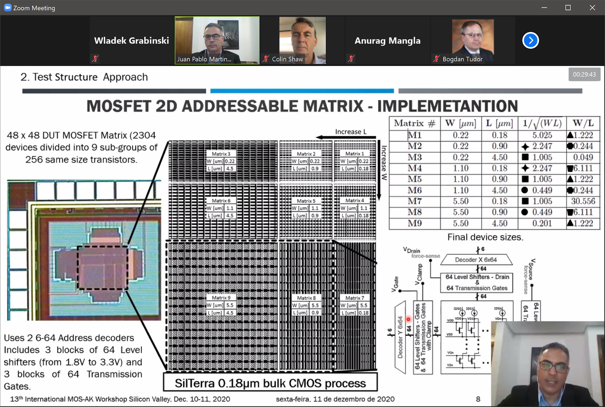
[8] Statistical Analysis of MOSFET extracted parameters for n-MOS mismatch modeling.
Juan Pablo Martinez Brito
CEITEC SA/UFRGS (BR)

[9] Rapid multiscale simulation of nanoscale MOSFETs: Is an interplay between compact models and NEGF possible?
Alexander Kloes
NanoP, THM University of Applied Sciences (D)


[10] The Effect of Non Rectangular MOS Channels in Modelling High Voltage Lateral MOS
Marco Sambi, Lorenzo Labate, Simona Cozzi, Nicola Holzer
STMicroelectronics (I)

MOS-AK session IV
Chair: Daniel Tomaszewski, Lukasiewicz - IMiF, Warsaw (PL)

[11] Nonlinear Embedding Model for the Accelerated Design of PAs with the ASM-HEMT model
Patrick Roblin*, Miles Lindquist*, Nicholas Miller+ and Marek Mierzwinski^
*The Ohio State University, AFRL+, Keysight Corp.^ (USA)

[12] New analytical model for AOSTFTs
Antonio Cerdeira, Yoanlys Hernandez-Barrios, Magali Estrada, Benjamin Iniguez
CINVESTAV (MX) and URV (SP)

[13] Unifying the Modeling of Charge Trapping in RTN, 1/f Noise and BTI
Gilson Wirth
UFRGS (BR)

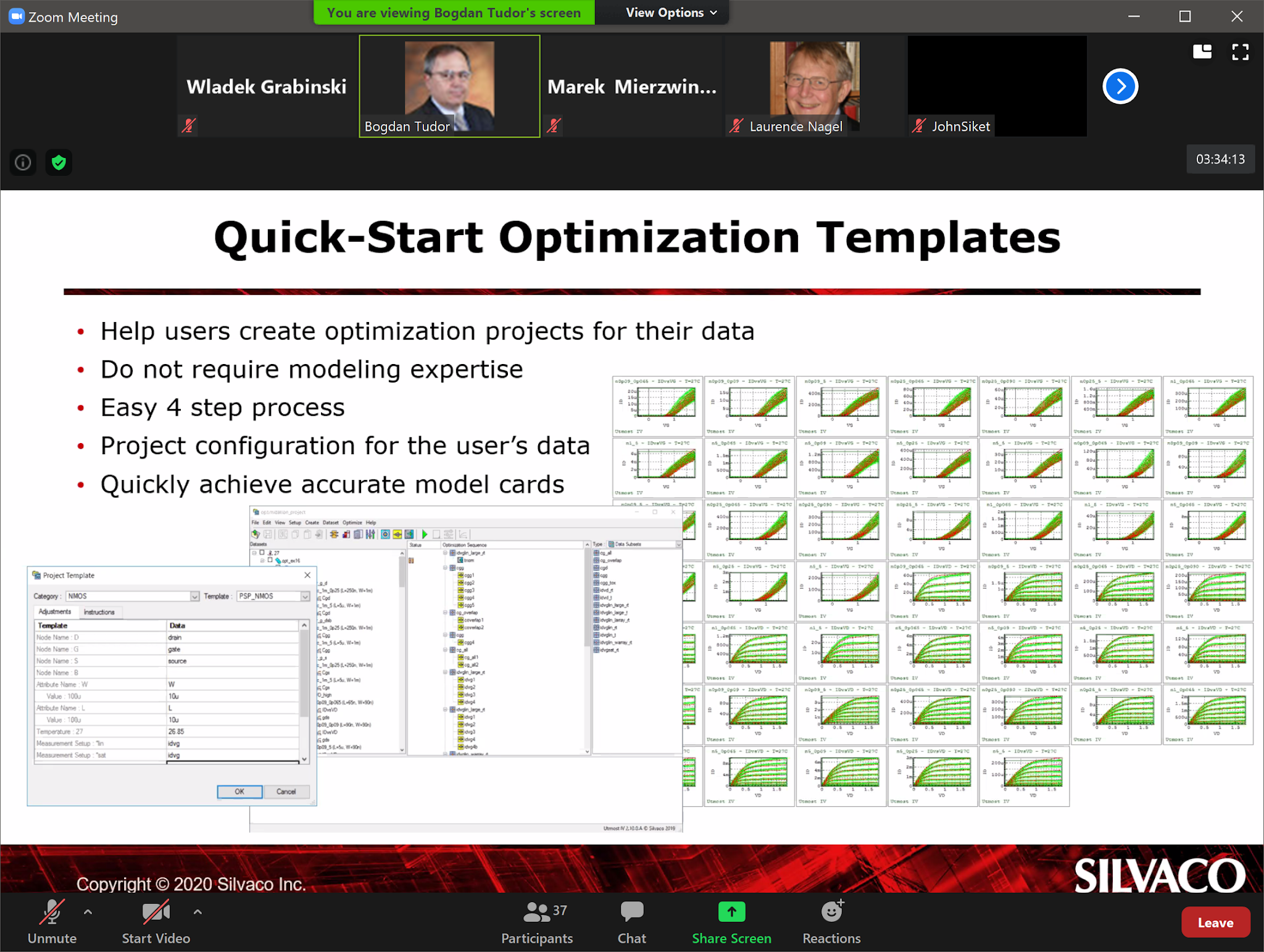
[14] SPICE Modeling for Display Technologies
Bogdan Tudor
Silvaco (USA)

MOS-AK attendees group photo of 2nd MOS-AK workshop day:

MOS-AK attendees group photo (1)

MOS-AK attendees group photo (2)