#Korean researchers 3D print highly-sensitive, #wearable #biosensors https://t.co/ZnXxlGvSfS#paper pic.twitter.com/7t2rVVC07n
— Wladek Grabinski (@wladek60) May 27, 2020
from Twitter https://twitter.com/wladek60
May 27, 2020 at 01:44PM
via IFTTT

#Korean researchers 3D print highly-sensitive, #wearable #biosensors https://t.co/ZnXxlGvSfS#paper pic.twitter.com/7t2rVVC07n
— Wladek Grabinski (@wladek60) May 27, 2020
#EU and #Japan step up cooperation in #science, #technology and innovation https://t.co/710WckAuB6#Paper pic.twitter.com/XdoU4mjQ3D
— Wladek Grabinski (@wladek60) May 26, 2020

Open PhD Positions In The Eu-Funded Project "GREAT". Currently, there are still vacancies in Germany and France. You can find more information at: https://t.co/9I9kUDznV7
— Wladek Grabinski (@wladek60) May 26, 2020
AMO GmbH | https://t.co/GS5EmAINfr#paper pic.twitter.com/haPyrQLtG9

 |
| FIG: Scheme of the pillar drivers supporting evolution of the IoT into IoE andTactile Internet. Some relevant IoT technology enablers are indicated. |
 |
| FIG: Schematic diagram of commonly used PCM mushroom structure |


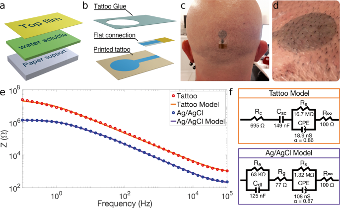 |
| Fig: Temporary tattoo electrodes (TTEs) for EEG: a The layered structure of the temporary tattoo paper permits the release of the top film on which electrodes are fabricated. b Expanded view of an all-polymer printed TTE. c A TTE released on the scalp, in Oz position. d Close-in view of a TTE released on the scalp after 12 h from application. e Impedance recordings on the forearm using TTE and Ag/AgCl electrodes. |
#EU Parliament Strongly Recommends Developing and Using #opensource Software https://t.co/6HxdUaUHQK pic.twitter.com/7czSKFmwh7
— Wladek Grabinski (@wladek60) May 19, 2020
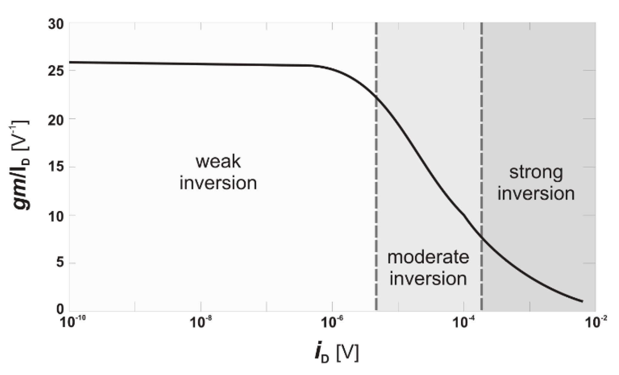 |
| Figure: gm/ID versus iD |
#Linux not #Windows: Why #Munich is shifting back from Microsoft to #opensource ...again https://t.co/7kCWSVHIOk pic.twitter.com/KVPAvUZr8o
— Wladek Grabinski (@wladek60) May 14, 2020
#paper: Smith, A.F., Liu, X., Woodard, T.L. et al. #Bioelectronic protein nanowire sensors for ammonia detection. Nano Res. (2020)https://t.co/eTvrtblGS0
— Wladek Grabinski (@wladek60) May 14, 2020
A new, highly sensitive #chemical #sensor uses protein nanowires https://t.co/lj2MoELcLp pic.twitter.com/03cHA6MNIc
#OpenRAMAN: #OpenSource Raman Spectrometer Is Cheaper, But Not Cheap https://t.co/SAKV61rdou pic.twitter.com/SotKelrOVK
— Wladek Grabinski (@wladek60) May 13, 2020
 |
| Fig: Log shifter implemented in CiM-HE. |

 |
| FIG: Schematic of the LDMOS. Lightly doped n-region constitutes the drain. Majority of the applied drain voltage drops across this region, which protects the intrinsic transistor region from breakdown. |
 |
| Fig: Simulation of a novel floating - gate synaptic transistor. (a) Device structure with separate negative feedback gate (nfb) for programming and synaptic gate (sg) readout. (b) Equivalent circuit diagram for compact modeling |
 |
| Fig: 2D sketch of the n-type DG TFET device geometry, showing the channel thickness t ch , the channel length l ch , the gate oxide thickness tox and the length of the S/D region l sd . Source (S) and drain (D) region are highly p/n-doped with a doping concentration N s/d |