Showing posts with label Analytical Model. Show all posts

Dec 8, 2021

[paper] Analytical Compact Model Of Cylindrical Junctionless Nanowire FETs

Adelcio M. de Souza, Daniel R. Celino, Regiane Ragi, Murilo A. Romero
Fully analytical compact model for the Q–V and C–V characteristics 
of cylindrical junctionless nanowire FETs
Microelectronics Journal (2021): 105324
DOI: 10.1016/j.mejo.2021.105324
   
University of Sao Paulo (EESC/USP), Sao Carlos (BR)

Abstract: This paper develops a new compact model for the Q–V and C–V characteristics of cylindrical junctionless nanowire FETs in which the nanowire radius is large enough, in such a way that quantum confinement effects can be neglected. Our model is fully analytical and valid for all bias regimes, i.e., subthreshold, partial depletion, and accumulation. The obtained Q-V and C–V characteristics, as well as their derivatives, are continuous across the full range of bias voltages. The model is fully physics-based, with no fitting parameters, and it is very intuitive, since it relies on the understanding of the device as a gated resistor. Model validation is performed against previous results in the literature, demonstrating very good agreement.
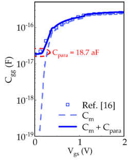
Fig.  Validation of our C–V model (solid lines) in comparison to numerical results, highlighting the effect of parasitic capacitance. The free-carrier capacitance component from new model is shown in dashed lines. Simulation parameters: tox = 4.5nm, Nd = 1.6E18 cm−3, L = 200nm, VFB = 1.09V and Vds = 0.05V.

Acknowledgments: The authors would like to thank the Brazilian funding agencies CAPES, CNPq, and Fapesp for their financial support: Conselho Nacional de Desenvolvimento Científico e Tecnologico. Grant Number: 303708/2017-4; Coordenaçao de Aperfeiçoamento de Pessoal de Nível Superior; Fundaçao de Amparo a Pesquisa do Estado de Sao Paulo. Grant Number: 18/13537-6.

Jul 22, 2020

[paper] Unified Analytical Model for SOI LDMOS

Baoxing Duan, Jingyu Xing, Ziming Dong and Yintang Yang1 (Senior Member, IEEE)
Unified Analytical Model for SOI LDMOS With Electric Field Modulation
IEEE J-EDS, vol. 8, pp. 686-694, 2020
DOI: 10.1109/JEDS.2020.3006293

1Key Laboratory of the Ministry of Education for Wide Band-Gap Semiconductor Materials and Devices, School of Microelectronics, Xidian University, Xi’an 710071, China

Abstract: The unified analytical model is proposed for SOI LDMOS (Silicon On Insulator Lateral Double-diffused Metal Oxide Semiconductor) based on the electric field modulation in this paper for the first time. The analytical solutions of the surface electric field distributions and potential distributions are derived on the basis of the 2-D Poisson equation. The variation of the buried layer parameters modulates the surface electric field by the electric field modulation effect to optimize the surface electric field distribution of the device. Also, the simulation results obtained through the simulation software ISE are consistent with the expected results of the analytical model. This not only proves the feasibility of the electric field modulation theory, but also shows that the accurate analytical model will be of great guiding significance for designing and optimizing the same LDMOS based on SOI structures.
FIG: Cross-sectional view of electric field modulated SOI LDMOS

Acknowledgment: This work was supported in part by Science Foundation for Distinguished Young Scholars of Shaanxi Province under Grant 2018JC-017, and in part by the 111 Project under Grant B12026.

May 25, 2020

[paper] Graphene/4H-SiC/Graphene MSM UV-photodetector


An optimized Graphene/4H-SiC/Graphene MSM UV-photodetector operating
in a wide range of temperature 
H. Bencherif 1, L. Dehimi1 2, G. Messina 3, P. Vincent 4, F. Pezzimenti 3, F. G. Della Corte 3 1Laboratory of Metallic and Semiconductor Materials, University of Biskra, Biskra, DZ
2Faculty of Science, University of Batna 1, DZ
3DIIES, Mediterranea University of Reggio Calabria, Reggio Calabria, IT
4School of Electronics Engineering, KNU, 80 Daehakro, Buk-gu, Daegu, 702-701, KP

Abstract: In this paper, .an accurate analytical model has been developed to optimize the performance of an Interdigitated Graphene Electrode/p-silicon carbide (IGE/p-4H-SiC) Metal semiconductor Metal (MSM) photodetector operating in a wide range of temperatures. The proposed model considers different carrier loss mechanisms and can reproduce the experimental results well. An overall assessment of the electrodes geometrical parameters’ influence on the device sensitivity and speed performances was executed. Our results confirm the excellent ability of the suggested Graphene electrode system to decrease the unwanted shadowing effect. A responsivity of 238 μA/W was obtained under 325-nm illumination compared to the 16.7 μA/W for the conventional Cr-Pd/p-SiC PD. A photocurrent to- dark-current ratio (PDCR) of 5.75 × 10⁵ at 300K and 270 at 500K was distinguished. The response time was found to be around 14 μs at 300K and 54.5 μs at 500K. Furthermore, the developed model serves as a fitness function for the multi objective optimization (MOGA) approach. The optimized IGE/p-4H-SiC MSM-PD design not only exhibits higher performance in terms of PDCR (7.2×10⁵), responsivity (430A/cm2) and detectivity (1.3×10¹⁴ Jones) but also balances the compromise between ultrasensitive and high-speed figures of merit with a response time of 4.7 μs. Therefore, the proposed methodology permits to realize ultra-sensitive, high-speed SiC optoelectronic devices for extremely high temperature applications. 
FIG: a) Energy band diagram of Graphene/p-SiC/Graphene structure, b) Cross-sectional view of the suggested IGE/4H-SiC MSM UV-PD with interdigitated electrodes

Acknowledgments: This work was supported by DGRSDT Of Ministry of Higher education of Algeria. The work was done in the unit of research of materials and renewable energies (URMER).