Oct 19, 2020

#Dialog Semiconductor Licenses its #Non-Volatile #Resistive #RAM Technology to #GF for 22FDX Platform, Targeting IoT and AI https://t.co/ReWiCM4oCv #semi https://t.co/o7CMYt9HkV


from Twitter https://twitter.com/wladek60

October 19, 2020 at 05:44PM
via IFTTT

[paper] Single Gate Extended Source Tunnel FET

Jagritee Talukdara, Gopal Rawatb, Bijit Choudhuria, Kunal Singhc, Kavicharan Mummanenia
Device Physics Based Analytical Modeling for Electrical Characteristics of Single Gate Extended Source Tunnel FET (SG-ESTFET)
Superlattices and Microstructures (2020): 106725
DOI: 10.1016/j.spmi.2020.106725

aDECE, NIT Silchar, Assam, India
bDECE, NIT Hamirpur, Himachal Pradesh, India
cDECE, NIT Jamshedpur, Jharkhand, India

Abstract: In this paper, a 2D analytical model for Single Gate Extended Source Tunnel FET has been developed which is based on the solution of Poisson’s equation simplified using parabolic approximation method. Different electrical characteristics of device physics such as surface potential, drain current, lateral, and vertical electric field of SG-ESTFET are studied incorporating various parameters like mole fraction of SiGe layer, gate dielectric constants, etc. Furthermore, in modeling and simulation, the depletion region of the drain side is included considering the effect of the fringing field. The comercial TCAD device simulator has been used to verify the accuracy and validity of the proposed analytical model for various electrical parameters such as gate to source voltage, mole fraction, and gate dielectric constants. The validity of the proposed model is confirmed by observing a decent agreement between modeling and simulation. The proposed compact model delivers quick and accurate values of various performance parameters.
Fig: 2D schematic device structure of SG-ESTFET


[paper] Parameter Extraction Technique for IGBT Compact Model

N.V. Bharadwaj1, Dr. P. Chandrasekhar2 and Dr. M. Sivakumar3
A Consecutive Parameter Extraction Technique for IGBT Compact Model
ICMM-2019; AIP Conf. Proc. 2269, 030031-1–030031-5;
DOI: 10.1063/5.0019484

1Geethanjali College of Enegineering and Technology, Hyderabad, 501301, India 
2MGIT, Hyerabad, 500075, India 
3Gudlavalleru Engineering College, Gudlavalleru , 521356, India

Abstract: A consecutive parameter extraction technique describes the fitting target related parameters for Insulated-gate bipolar transistor (IGBT) model. The IGBT model has been represented by a couple of simplified equivalent circuits. Using simulated data for a trench-type IGBT as reference the performance of compact model IGBT is compared to an IGBT macro model. Due to physics based modeling, parameter extraction with the compact model is fast. With very less extraction effort, the compact model fits the dc current and capacitance characteristics accurately.

FIG: The IGBT cell structure with cell pitch = 4μm and trench gate depth = 3μm


#China Forecast to Represent 22% of the #Semi #Foundry Market in 2020


from Twitter https://twitter.com/wladek60

October 19, 2020 at 09:25AM
via IFTTT

Oct 16, 2020

#SIA and #SRC publish $3.4bn plan for stimulating #US #semi R&D


from Twitter https://twitter.com/wladek60

October 16, 2020 at 04:52PM
via IFTTT

Oct 15, 2020

Emerging Technologies Initiative (ETI)

Emerging Technologies Initiative (ETI)


What are classified as emerging technologies?
Emerging technologies have the potential to disrupt many existing industries and significantly impact employment, security, social equity, and global relations. However, it is important to note that disruptive innovations are not just a result of new technologies.  Incremental innovations in products and processes or aggregation of clustering of technologies can also combine to result in disruptive innovation – as seen recently in the case of several FinTech and AgriTech applications. 
For the purpose of this initiative, an indicative list of technologies are given below for the reference (including but not limited to):

What are the expected outcomes of ETI?
  • Develop a critical mass of individuals/groups who are interested in thinking at the intersection of ‘Science & Technology’ and ‘International Engagement’
  • Identify and prioritize the technologies of relevance and importance (present as well as future)
  • Map technology and innovation hubs in India to anticipate the policy implications of the latest developments in emerging technologies
  • Build a comprehensive Technology Intelligence Database (TID) for identified technologies. 
  • Provide evidence-informed policy choices and program roadmaps for technology indigenization (reducing tech dependency and increasing domestic tech intensity)   
  • Develop and strengthen the tech-knowledge capacity of central and state ministries, departments,  industries, accelerators and startups with the help of TID.
  • Operationalize the technology indigenization roadmaps with identified stakeholders onboard
  • Act as a synapsis amongst different stakeholders by facilitating the exchange of knowledge, expertise, and services to develop the emerging technology ecosystem.

Partners:
  • The Office of the Principal Scientific Adviser to the Government of India (Office of PSA)
  • New Emerging & Strategic Technologies Division in the Ministry of External Affairs (NEST, MEA #NESTMEA)
  • Science Policy Forum (SPF)


[paper] Scaled GaN-HEMT Large-Signal Model Based on EM Simulation

Scaled GaN-HEMT Large-Signal Model Based on EM Simulation
Wooseok Lee1, Hyunuk Kang1, Seokgyu Choi2, Sangmin Lee2, Hosang Kwon3, Keum cheol Hwang1, Kang-Yoon Lee1 and Youngoo Yang1
Electronics 2020, 9(4), 632
DOI: 10.3390/electronics9040632
1Department of Electrical and Computer Engineering, Sungkyunkwan University, Suwon 16419, Korea
2Wavice Inc., Hwaseong-si 18449, Korea
3Agency for Defense Development, Daejeon 34186, Korea

Abstract This paper presents a scaled GaN-HEMT large-signal model based on EM simulation. A large-signal model of the 10-finger GaN-HEMT consists of a large-signal model of the two-finger GaN-HEMT and an equivalent circuit of the interconnection circuit. The equivalent circuit of the interconnection circuit was extracted according to the EM simulation results. The large-signal model for the two-finger device is based on the conventional Angelov channel current model. The large-signal model for the 10-finger device was verified through load-pull measurement. The 10-finger GaN-HEMT produced an output power of about 20 W for both simulation and load-pull measurements. 
Fig: Two-finger GaN-HEMT: a) layout; b) equivalent SPICE subcircuit

Acknowledgement: The research reported in this work has been supported by ADD (Agency of Defense Development) of Korea under an R&D program (UC170025FD).


[webinar] GaN HEMT Devices Characterization Using ASM-HEMT Model

ASM-HEMTモデルを使ったGaN HEMTデバイスの特性評価とモデリング


お知らせ: キーサイト・テクノロジーのウェブセミナー「ASM-HEMTモデルを使ったGaN HEMTデバイスの特性評価とモデリング 」

ライブウェブセミナーの日付: 2020年10月14日
ライブウェブセミナーの時刻: 10:45 JST

The Evolution of SPICE Continues With PSPICE for TI https://t.co/gBbrLEU2NJ #semi https://t.co/moYCCqfd1Y


from Twitter https://twitter.com/wladek60

October 15, 2020 at 12:16PM
via IFTTT

Oct 14, 2020

[C4P] ICMTS: April 12 - 15, 2021

34th International Conference on Microelectronic Test Structures
ICMTS: April 12 - 15, 2021
Crowne Plaza Cleveland at Playhouse Square, Cleveland, OH, USA

Looking for the best opportunity to present and discuss your ideas and results about test structures, measurements and characterization? This is your chance! Join the 34th ICMTS conference. A Tutorial Short Course will precede the main conference. Several of the best measurement, equipment design, and manufacturing experts, will participate in the equipment exhibition and presentations. The conference will bring together designers and users of test structures to discuss recent developments and future directions, in a one-track program, with convivial breaks allowing attendees to discuss and exchange viewpoints and challenges. A Best Paper award will be presented by the Technical Program Committee. The IEEE Electron Devices Society is the co-sponsor, and all presented papers will be submitted for possible inclusion on IEEE Xplore®. Original papers are solicited presenting new developments in topics relevant to ICMTS, including but not limited to, test structures, measurements, and results, in the following areas:
  • Design
    • Methodologies, verification
    • Within-die circuits for process characterization/monitoring
    • Design enablement – Characterization and validation of digital and analog libraries
  • Measurement techniques
    • DC, AC and RF measurements: setup, test and analysis
    • Reliability test - including thermal stability, failure analysis etc.
    • Statistical analysis, variability, throughput increase, smart test strategies
    • Use of machine learning and AI in analysis of data sets - parameter extraction etc.
    • Wafer probing, within-die measurements, in-line metrology
    • Throughput, testing strategies, yield enhancement and process control tests
  • Applications
    • Emerging memory technologies (single cell, arrays, and application in neural networks)
    • Emerging transistor technologies for digital/analog/power applications
    • Photonic devices - silicon integration, new displays (OLED, µ-displays)
    • Flexible electronics and sensors (organic and inorganic materials)
    • M(N)EMS, actuators, sensors, PV cells and other emerging devices
The author’s abstract submission consists of up to four pages in PDF format (font-embedded). The first page should include a title, a 50-word summary, author name(s), full address, contact number, and e-mail of the lead author, and any preference for oral or poster session presentation. The body of the abstract should consist of one page of text (800 to 1000 words) and up to two pages of major figures and tables. The selection process will be based on the technical merit and will be highly weighted in favor of abstracts with high test structure content (including illustration) along with measurements and data analysis.

The abstract submission deadline is November 6, 2020.

Abstracts can be submitted via the ICMTS website http://www.icmts.net using the “Submit Abstract” link on the front page. Notice of paper acceptance will be sent to the selected authors by mid-January, 2020, with instructions for the expanded manuscript preparation for the conference proceedings. The deadline for submission of the final paper will be March 17, 2021. 

Please join the ICMTS group at www.linkedin.com/groups/3804498, if you have in interest all things test structure related.

Details of the venue, hotel, registration, etc. will be posted at the ICMTS official web site. ICMTS is currently planned to be in person with the possibility of going virtual if necessary.

For further technical information, please contact the technical program chair:Chadwin Young, University of Texas at Dallas.

General Chair:
Brad Smith NXP Semiconductors
Technical Program Chair:
Chadwin Young University of Texas, Dallas
Tutorial Chair:
Matthew Rerecich Samsung Austin Semiconductor, LLC
Equipment Exhibition Chair:
Garrett Tranquillo Celadon Systems, Inc.
Local Arrangements:
Brad Smith NXP Semiconductors

ICMTS Steering Committee:
Asian Representative:
Satoshi Habu Keysight Technologies, Japan
European Representative:
Hans Tuinout NXP Semiconductors
USA Representative:
Bill Verzi Semiconductor Test Advisor


[online] PhD Thesis Colloquium of student Mr. Biswapriyo Das


FROM: Professor Santanu Mahapatra ( শান্তনু মহাপাত্র ) 
Nano Scale Device Research Laboratory
Department of Electronic Systems Engineering (formerly CEDT)
Indian Institute of Science Bangalore
Bangalore 560012 INDIA

Dear Colleagues, 
Hope you are in good health amid this pandemic.

I would like to invite you and your team members to the online thesis colloquium of my PhD student Mr. Biswapriyo Das. In our institute, it is mandatory for a PhD student to give an open colloquium for his research work just before the thesis submission. In pre-COVID time, it used to be a physical presentation, attended by the institute community. However, during this evolving pandemic we are conducting the colloquium online. It thus gives us opportunity to invite researchers across the globe who are working on the similar problems in device-modeling .

You may find the details of the talk below. Hope to see you and your group members on 19th October at 3PM IST. MS Teams Link:
https://teams.microsoft.com/l/meetup-join/19%3ameeting_MjhmYzJiYjAtNzY2Zi00OGU5LWFhMzgtODQyYmJmNjAzYzhl%40thread.v2/0?context=%7b%22Tid%22%3a%226f15cd97-f6a7-41e3-b2c5-ad4193976476%22%2c%22Oid%22%3a%228c0cf3c3-0cab-451f-a745-7b29517ae80f%22%7d

Title:  Atom-to-circuit modeling strategy for 2D transistors

Abstract: Two-dimensional (2D) materials are now being considered as viable options for CMOS (complementary metal-oxide-semiconductor) technology extension due to their diverse electronic and opto-electronic properties. However, introduction of any new material in the process integration phase of technology development in semiconductor industry is an expensive and time-consuming affair. It is also a difficult task to select an appropriate 2D material from the plethora without assessing their performance at circuit level. Thus, first-principles-based multiscale models that enable systematic performance evaluation of emerging 2D materials at device and circuit levels solely from their crystallographic information is in great demand. In this thesis, such an atom-to-circuit modeling framework, addressing three different levels of abstraction (viz. material, device and circuit), has been demonstrated.
Firstly, the model was implemented for a van der Waal's heterostructure based all-2D metal-insulator-semiconductor field-effect transistor (MISFET), comprising of vertically stacked semi-metallic graphene, insulating hexagonal boron nitride (hBN) and semiconducting monolayer molybdenum disulphide (MoS­2). Our physics-based compact model demonstrates the effects of band gap opening in graphene due to its sublattice symmetry breaking interactions with underlying hBN layer. This apart, we have also studied the effects of semiconductor doping and the band gap variation of graphene at device and circuit levels. The model equations were thereafter implemented in a professional circuit simulator using its Verilog-A interface to facilitate design and simulation of integrated circuits.
Secondly, the scope of the proposed model was further extended to capture the non-quasi-static (NQS) effects in 2D transistors operating at very high frequencies, typically greater than its intrinsic cut-off frequency fT. Taking phosphorene as a prototypical example, a multiscale NQS model was developed for 2D transistors that can predict the channel-orientation-dependent high-frequency performance of devices and circuits solely from the crystallographic information of their constituent materials. The material-specific parameters obtained from density functional theory (DFT) calculations were used to develop a continuity equation based NQS model to gain insight into the high-frequency behaviours. It was found that channel orientation has strong impact on both the low and high frequency conductances, however it affects only the high-frequency component of capacitances. The model was then implemented in industry-standard circuit simulator using relaxation-time-approximation technique and simulations of analog and digital circuits were carried out to demonstrate its applicability for near cut-off frequency circuit operation.
Finally, the idea was also exercised for modeling novel quantum materials like 2D topological insulators (TI) and it was shown that the proposed analytical approach could be useful for developing compact models of topological insulator field effect transistors. A k. p Hamiltonian based continuum model was used to unveil the bandgap opening in the edge-state spectra of finite-width monolayer 1T' molybdenum disulphide (MoS2), molybdenum diselenide (MoSe2), tungsten disulphide (WS2) and tungsten diselenide (WSe­2). It was shown that the application of a perpendicular electric field effectuates a topological phase transition and it can simultaneously modulate the band gaps of both bulk and edge-states. The tuneable edge conductance, as obtained from the Landauer-Büttiker formalism, exhibits a monotonous increasing trend with applied electric field for deca-nanometer MoS­2, whereas the trend is opposite for other cases.

References:
[1] Das, B. and Mahapatra, S., "An atom-to-circuit modeling approach to all-2D metal-insulator-semiconductor field-effect transistors", npj 2D Mater Appl 2, 28 (2018).
[2] Das, B., Sen, D. and Mahapatra, S., "Tuneable quantum spin Hall states in confined 1Tʹ transition metal dichalcogenides", Sci Rep 10, 6670 (2020).
--------------------------------------------------------
Santanu Mahapatra ( শান্তনু মহাপাত্র )
Professor
Nano Scale Device Research Laboratory
Department of Electronic Systems Engineering (formerly CEDT)
Indian Institute of Science Bangalore
Bangalore 560012 INDIA

Adjunct Faculty IIIT-Allahabad

Phone: +91-80-2293-3090
Home Page: santanu.dese.iisc.ac.in
Lab Page: nsdrl.dese.iisc.ac.in


--
You received this message because you are subscribed to the Google Groups "mos-ak" group.
To unsubscribe from this group and stop receiving emails from it, send an email to mos-ak+unsubscribe@googlegroups.com.
To view this discussion on the web visit https://groups.google.com/d/msgid/mos-ak/CALp-Rj9c2QXCsyYYwLoDMZxRkZgyTy1ME83tDnYNMCqhSDBZLw%40mail.gmail.com.

Oct 13, 2020

[C4P] Special Issue "Smart Sensors for Wearable Applications" Keywords: Mobile health technology, Wearable technology, Smart sensors, Flexible and stretchable sensors, Optic sensors, Healthcare and wellness, IoT, Brain mapping https://t.co/EgX32M9eF2 #semi https://t.co/AwrzJ6qiYh


from Twitter https://twitter.com/wladek60

October 13, 2020 at 05:15PM
via IFTTT

SOT-MRAM Startup Raises $11M to Achieve Scalability [EE Times Europe] https://t.co/TDMt5YKLOM #semi https://t.co/5Bic8ShFqg


from Twitter https://twitter.com/wladek60

October 13, 2020 at 10:35AM
via IFTTT

[paper] TFETs for sensitive THz detection

I. Gayduchenko1,2, S.G. Xu3,4, G. Alymov1, M. Moskotin2,1, I. Tretyakov5, T. Taniguchi6, K.Watanabe7, G. Goltsman8, A.K. Geim3,4, G. Fedorov1,2, D. Svintsov1, and D.A. Bandurin3,1
Tunnel field-effect transistors for sensitive terahertz detection
arXiv:2010.03040 (2020)

1Moscow Institute of Physics and Technology (National Research University), Dolgoprudny 141700, Russia
2Physics Department, Moscow Pedagogical State University, Moscow, 119435, Russia
3School of Physics, University of Manchester, Oxford Road, Manchester M13 9PL, United Kingdom
4National Graphene Institute, University of Manchester, Manchester M13 9PL, United Kingdom
5Astro Space Center, Lebedev Physical Institute of the Russian Academy of Sciences, Moscow 117997, Russia
6International Center for Materials Nanoarchitectonics, National Institute of Material Science, Tsukuba 305-0044, Japan
7Research Center for Functional Materials, National Institute of Material Science, Tsukuba 305-0044, Japan
8National Research University Higher School of Economics, Moscow, 101000, Russia


Abstract: The rectification of high-frequency electromagnetic waves to direct currents is a crucial process for energy harvesting, beyond 5G wireless communications, ultra-fast science, and observational astronomy. As the radiation frequency is raised to the sub-terahertz (THz) domain, efficient ac-to-dc conversion by conventional electronics becomes increasingly challenging and requires alternative rectification protocols. Here we address this challenge by tunnel field-effect transistors made of dual-gated bilayer graphene (BLG). Taking advantage of BLG’s electrically tunable band structure, we create a lateral tunnel junction and couple it to a broadband antenna exposed to THz radiation. The incoming radiation is then down-converted by strongly non-linear interband tunneling mechanisms, resulting in exceptionally high-responsivity (exceeding 3kV/W) and low-noise (0.2pW/Hz detection at cryogenic temperatures. We demonstrate how the switching from intraband Ohmic to interband tunneling regime within a single detector can raise its responsivity by one order of magnitude, in agreement with the developed theory. Our work demonstrates an unexpected application of interband tunnel transistors for high-frequency detection and reveals bilayer graphene as one of the most promising platforms therefor.
Fig: Overview of THz detectors. NEP for THz detectors of various types plotted against the temperature at which they operate. Vertical error bars represent the spread of the detectors’ performance over the frequency range 0.1−2 THz. Horizontal error bars show the temperature range at which the detectors operate.  

Acknowledgements: This work was supported by the Russian Foundation for Basic Research within Grants No. 18-37-20058 and No. 18-29-20116. Experimental work of IG (photoresponse measurements) was supported by the Russian Foundation for Basic Research (grant 19-32-80028). We acknowledge support of the Russian Science Foundation grant No. 19-72-10156 (NEP analyses) and grant No.17-72-30036 (transport measurements). The work of GA and DS (theory of THz detection) was supported by grant # 16-19-10557 of the Russian Scientific Foundation. K.W. and T.T. acknowledge support from the Elemental Strategy Initiative conducted by the MEXT, Japan, Grant Number JPMXP0112101001, JSPS KAKENHI Grant Number JP20H00354 and the CREST(JPMJCR15F3), JST. The authors thank A. Lisauskas, W. Knap, A. I. Berdyugin and M.S. Shur for helpful discussions.

Oct 12, 2020

[paper] Compact Modeling of GaN HEMTs

Y. Chen et al., "Compact Modeling of THZ Photomixer Made from GaN HEMT," 2020 IEEE International Conference on Advances in Electrical Engineering and Computer Applications (AEECA), Dalian, China, 2020, pp. 484-489, doi: 10.1109/AEECA49918.2020.9213681.

Y. Chen et al., "A Surface Potential Based Compact Model for GaN HEMT I-V and CV Simulation," 2020 IEEE International Conference on Advances in Electrical Engineering and Computer Applications (AEECA), Dalian, China, 2020, pp. 490-495, doi: 10.1109/AEECA49918.2020.9213674.

A. Zhang et al., "Compact Modeling of Capacitance Components for GaN HEMTs," 2020 IEEE International Conference on Advances in Electrical Engineering and Computer Applications (AEECA), Dalian, China, 2020, pp. 505-511, doi: 10.1109/AEECA49918.2020.9213571.


FIG: Simplified GaN HEMT Structure


[chapter] Low-Voltage Analog IC Design

Deepika Gupta1
Low-Voltage Analog Integrated Circuit Design
Nanoscale VLSI. Book series (ESIEE) (2020) pp 3-22
DOI: 10.1007/978-981-15-7937-0_1
1Department of Electronics and Communication Engineering, IIIT Naya Raipur, India

Abstract: In this chapter, we review the challenges and effective design techniques for ultra-low-power analog integrated circuits. With the miniaturization, having low-power low-voltage mixed signal IC is essential to maintain the electric field in the device. This constraint presents bottleneck for the researchers to design robust analog circuits. Specifically, the low value of supply voltage with small technology influences many specifications of analog IC, e.g., power supply rejection, dynamic range and immunity to noise, etc. In addition, it also affects the ability of the MOS transistor to be operated in the strong inversion region. Note that with the technology reduction, power supply VDD is reducing but the threshold voltage VT is not decreasing proportionally to maintain low leakage current. However, this process reduces the overdrive voltage and limits the staking of transistors. In this case, the transistor can be made to work in weak inversion to work and reduce the power consumption. Further, reduction in VDD to achieve low-power consumption causes many other circuit-related issues such as PVT variations, degradation of dynamic range, mismatching in circuits element and differential paths. There have been many design methods developed for the ultra-low-power analog ICs. In this chapter, we will discuss some of the design techniques to reduce the power consumption in analog ICs. In addition, we will also discuss the basic building blocks of analog circuits with discussed design techniques. The charge-based EKV model can be a very suitable example of a MOS simulation model to be used in all inversion regions of transistor operations [Enz 2017]. In EKV model, the smallest number of core parameters is needed for the accurate behavioral modeling of transistor. Particularly, charge-based EKV model is beneficial for the analysis of analog circuits because it allows the analysis with simple calculations over different inversion regions. Hence, developing new device simulation models specific for analog circuit design is crucial.
Fig: Vth and Vdd scaling trend vs. Leff  [Zhao 2006]
References:
[Enz 2018] Enz C, Chicco F, Pezzotta A (2017) Nanoscale MOSFET modeling-part 1: the simplified EKV model for the design of low-power analog circuits. IEEE Solid-State Circuits Magazine 9(3):26–35
[Zhao 2006] Zhao W, Cao Y (2006) New generation of predictive technology model for sub-45 nm early design exploration. IEEE Trans Electron Devices 53(11):2816–2823


Oct 9, 2020

[paper] TCAD-Machine Learning Framework

Hiu Yung Wong1 (Senior Member, IEEE), Ming Xiao2, Boyan Wang2, Yan Ka Chiu1, Xiaodong Yan3, Jiahui Ma3, Kohei Sasaki4, Han Wang3 (Senior Member, IEEE)
and Yuhao Zhang2 (Member, IEEE)
TCAD-Machine Learning Framework for Device Variation and Operating Temperature Analysis with Experimental Demonstration
IEEE J-EDS, vol. 8, pp. 992-1000, 2020
doi: 10.1109/JEDS.2020.3024669.

1Department of Electrical Engineering, San Jose State University, San Jose, CA 95112, USA
2Virginia Polytechnic Institute, State University, Blacksburg, VA 24060, USA
3Ming Hsieh Department of Electrical Engineering, University of Southern California, Los Angeles, CA 90089, USA
4Development Department, Novel Crystal Technology Inc., Sayama 3501328, Japan

Abstract: This work, for the first time, experimentally demonstrates a TCAD-Machine Learning (TCADML) framework to assist the analysis of device-to-device variation and operating (ambient) temperature without the need of physical quantities extraction. The ML algorithm used in this work is the Principal Component Analysis (PCA) followed by third order polynomial regression. After calibrated to limited ‘expensive’ experimental data, ‘low cost’ TCAD simulation is used to generate a large amount of device data to train the ML model. The ML was then used to identify the root cause of device variation and operating temperature from any given experimental current-voltage (I-V) characteristics. We applied this framework to study the ultra-wide-bandgap gallium oxide (Ga2O3) Schottky barrier diode (SBD), an emerging device technology that holds great promise for temperature sensing, RF, and power applications in harsh environments. After calibration, over 150,000 electrothermal TCAD simulations are performed with random variation of physical parameters (anode effective work function, drift layer doping, and drift layer thickness) and operating temperature. An ML model is trained using these TCAD data and we found 1,000-10,000 TCAD data can train an accurate machine. We show that without physical quantities extraction, performing PCA is essential for the TCAD trained ML model to be applicable to analyze experimental characteristics. The physical parameters and temperatures predicted by the ML model show good agreement with experimental analysis. Our TCAD-ML framework shows great promise to accelerate the development of new device technologies with a significantly more efficient process of material and device experimentation.


FIG: Flow chart diagram of the proposed TCAD-Machine Learning framework. All components are demonstrated in this article except the MLDatabase which stores previously trained ML algorithms.

Acknowledgment: The authors thank Dr. Pooya Jannaty of Cruise and Dr. Philip Leong of the University of Sydney for the discussion of ML algorithms. The experimental work is in part supported by the Southeastern Center for Electrical Engineering Education program and the High Density Integration industry mini-consortium of the Center for Power Electronics Systems at Virginia Tech.


[paper] Metamaterial for Wearable Applications

Kabir Hossain1,2, Thennarasan Sabapathy1,2, Muzammil Jusoh1,2, Ping Jack Soh11,2 Ainur Fasihah Mohd Fazilah1,2, Ahmad Ashraf Abdul Halim1,2, N. S. Raghava3, Symon K. Podilchak4, Dominique Schreurs5, Qammer H. Abbasi6
ENG and NZRI Characteristics of Decagonal Shaped Metamaterial for Wearable Applications
International Conference on UK-China Emerging Technologies 
UCET, Glasgow, United Kingdom, 2020, pp. 1-4, 
doi: 10.1109/UCET51115.2020.9205409

1Advanced Communication Engineering (ACE) Centre of Excellence, Universiti Malaysia Perlis, No 15 & 17, Jalan Tiga, Pengkalan Jaya Business Centre, 01000 Kangar, Perlis, Malaysia. 
2School of Computer and Communication Engineering, Universiti Malaysia Perlis, Kampus Alam UniMAP Pauh Putra, Arau 02600, Malaysia 
3Departments of Electronics and Communication Engineering, Delhi Technological University, India
4Institute of Digital Communications, School of Engineering, University of Edinburgh, EH9 3FB, UK
5ESAT-TELEMIC Research Division, KU Leuven, Kasteelpark Arenberg 10 Box 2444, 3001 Leuven, Belgium 
6James Watt School of Engineering, University of Glasgow, UK

Abstract: A decagonal-shaped split ring resonator metamaterial based on a wearable or textile-based material is presented in this work. Analysis and comparison of various structure sizes are compared considering a compact 6×6 mm2 metamaterial unit cell, in particular, where robust transmissionreflection (RTR) and Nicolson-Ross-Weir (NRW) methods have been performed to extract the effective metamaterial parameters. An investigation based on the RTR method indicated an average bandwidth of 1.39 GHz with a near-zero refractive index (NZRI) and a 2.35 GHz bandwidth when considering epsilon negative (ENG) characteristics. On the other hand, for the NRW method, approximately 0.95 GHz of NZRI bandwidth and 2.46 GHz of ENG bandwidth have been observed, respectively. These results are also within the ultrawideband (UWB) frequency range, suggesting that the proposed unit cell structure is suitable for textile UWB antennas, biomedical sensors, related wearable systems, and other wireless body area network communication systems.

Fig: The real NZRI values obtained using the RTR and NRW methods for different unit cell structures: (a) 1 1 × array, (b) 2 1× array, (c) 1 2 × array, and (d) 2 2 × array

Acknowledgment: The author would like to acknowledge the support from the Fundamental Research Grant Scheme (FRGS) under a grant number of FRGS/1/2019/TK04/UNIMAP/02/3 from the Ministry of Education Malaysia.

Oct 8, 2020

[paper] X-Parameters Based Characterization and Compact Modeling of SiGe HBT Linearity


from Twitter https://twitter.com/wladek60

October 08, 2020 at 05:22PM
via IFTTT

Special IJHSES Issue on Advancements in Smart Grid Technologies

0 cover

Call for Papers


Special Issue on Advancements in Smart Grid Technologies

This special issue is on electrical power generation, transmission, distribution and utilization in smart grid, from the viewpoints of individual power system elements and their integration, interaction and technological advancement.

The special issue focuses on microelectronic systems, circuits, power control and soft computing techniques in smart grid. It includes, but are not limited to, the following:

  • Renewable & Sustainable Energy Technologies
  • Cloud-assisted smart grid architectures and development
  • Internet-centric smart grid solutions
  • Case studies on recent advances in smart grid and renewable energy system
  • Information and communication technology for enhancing smart grid and renewable energy system
  • Future of renewable energy sources in environmental protection
  • Sustainable computational methods to evaluate the optimization of renewable energy systems
  • Networking and data mining in smart grids for continuous sustainable development
  • Threat, challenges & opportunity of integrating smart grid and renewable energy system
  • Generation techniques ranging from advances in conventional electromechanical methods, through nuclear power generation, to renewable energy generation.
  • A study on the smart grid and renewable energy system for reducing the complexity of power grids
  • Distribution techniques, equipment development, and smart grids.
  • Renewable power generation and clean energy technologies
  • Distributed energy resources and storage
  • Modern power grid devices, sensors and wireless technologies
Paper Submission and Review Schedule:
  • First announcement: October. 12th 2020
  • Submission Deadline: November30th 2020
  • Final notification: January 10, 2020
  • Publication Date: June 30th 2020

Camera ready articles should be sent to the Guest Editor for consideration. Please specify the research topic on the cover page.

IJHSES Editor-in-Chiefs:
Michael Shur, Rensselaer Polytechnic Institute (USA)
Wladek Grabinski, MOS-AK (EU)

Guest Editor:
Naresh Kumar YadavD.C.R.U.S.T, Murthal (India)

Oct 7, 2020

[paper] Flexible MO TFT for Analog Applications

Giuseppe Cantarella1, Júlio Costa2, Tilo Meister3, Koichi Ishida3, Corrado Carta3, Frank Ellinger3, Paolo Lugli1, Niko Münzenrieder1,2 and Luisa Petti1
Review of recent trends in flexible metal oxide thin-film transistors for analog applications
Flexible and Printed Electronics 2020, Vol. 5, No. 3
DOI: 10.1088/2058-8585/aba79a

1Faculty of Science and Technology, Free University of Bozen-Bolzano, 39100, Bozen, Italy
2Flexible Electronics Laboratory, University of Sussex, Brighton, BN1 9QT, United Kingdom
3Chair of Circuit Design and Network Theory, TU Dresden, 01069 Dresden, Germany

Abstract: Thanks to the extraordinary advances flexible electronics have experienced over the last decades, applications such as conformable active-matrix displays, ubiquitously integrated disposable flexible sensor nodes, wearable or textile-integrated systems, as well as imperceptible and transient implants are now reachable. To enable these applications, specialized analog circuits able to transmit and receive data, condition sensors' parameters, drive actuators or control powering devices are required. High-performance sensor conditioning, driving and transceiver circuits on a wide range of flexible substrates are therefore extremely important to develop. However, the currently available materials and processes compatible with mechanically flexible substrates impose massive limitations in terms of large-area uniformity, device dimensions' shrinkability and circuit design, challenging the realization of flexible analog systems. Among state-of-the-art technologies employing low-temperature fabrication processes, thin-film transistors (TFTs) based on metal oxide semiconductors represent the potentially best compromise in terms of prize, performance, technology maturity and capacity to realize complex systems. This is why metal oxide TFTs are nowadays widely used for flexible, light-weight, transparent, stretchable and bio-degradable analog circuits and systems. Here, we review the current trends of flexible metal oxide TFTs for analog applications. First, an introduction is given, where current challenges and requirements related to the realization of flexible analog circuits and systems are analysed. Additionally, TFT performance parameters and configurations are briefly revised. Then, the recent advances in the field of flexible metal oxide TFTs for analog applications are summarized. In particular, all reported approaches to reduce the channel length and improve the AC performance are shown. Next, the current state of flexible metal oxide TFT-based analog circuits is shown, discussing n-type only and complementary circuit configurations. The last topic of the review covers systems based on flexible metal oxide analog circuits. Finally, a conclusion is drawn and an outlook over the field is provided.

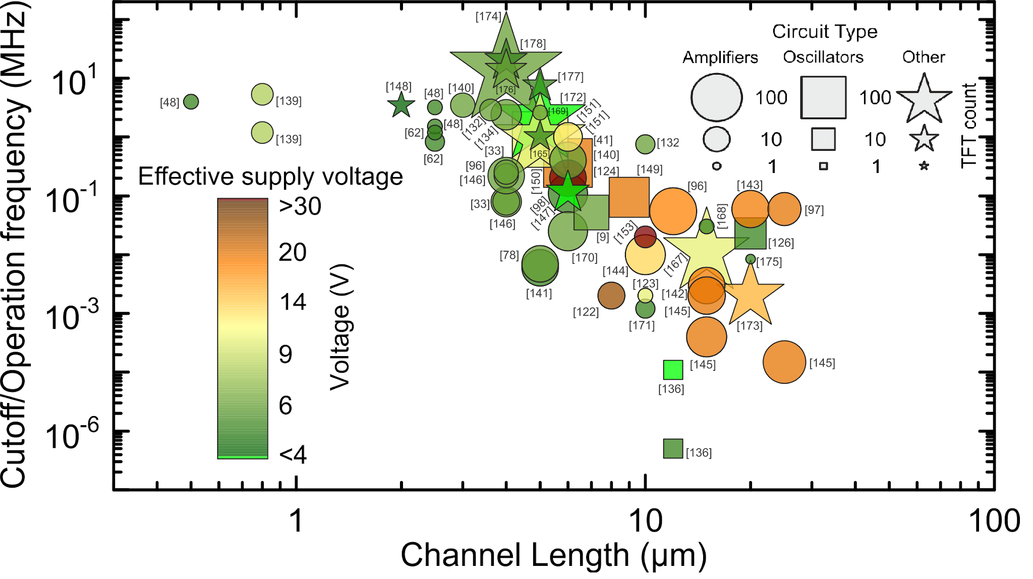
Figure: Overview of published works on flexible metal oxide TFT based circuits, indicating the minimum channel length of the devices, the operation frequency of the circuits, the effective supply voltage used, as well as the total TFT count. Only integrated circuits are included.

Acknowledgments: This work was partially supported by the DFG FFlexCom Priority Programme, Germany, through projects WISDOM II and Coordination Funds, under Grants 271795180 and 270774198. This work was also partially funded with internal funding of the Faculty of Science and Technology of the Free University of Bolzano-Bozen (project ”EYRE” RTD Call 2019).

[paper] Parameter Extraction in JFETs

Nikolaos Makris1, Matthias Bucher1, Member, IEEE, Loukas Chevas1, Farzan Jazaeri2
and Jean-Michel Sallese2
Free Carrier Mobility, Series Resistance, and Threshold Voltage Extraction
in Junction FETs
in IEEE Transactions on Electron Devices, 
Special Section on ESSDERC/ESSCIRC 2020
DOI: 10.1109/TED.2020.3025841.

1School of Electrical and Computer Engineering, TU Crete (GR)
2Ecole Polytechnique Fédérale de Lausanne, EPFL (CH)

Abstract: In this brief, extraction methods are proposed for determining the essential parameters of double gate junction field-effect transistors (FETs). First, a novel method for determining free carrier effective mobility, similar to a recently proposed method for MOSFETs, is developed. The same method is then extended to cover also the case when series resistance is present, while series resistance itself may be determined from the measurement from two FETs with different channel lengths. The key technological and design parameter is the threshold voltage, which may be unambiguously determined from the transconductance-to-current ratio with a constant-current method. The new methods are shown to be effective over a wide range of technical parameters, using technology computer-aided design simulations.

Fig: Extraction of carrier mobility for DG JFETs in linear region at 300K 
a) corresponding output conductance gds and constituents ∂gds/∂Vds and 2Qsc,d/b, and 
b) extracted mobility for long- and moderate-length devices close agreement with the constant, nonfield-dependent mobility (μ = 826 cm2/Vs) used in the TCAD simulations.

Aknowlegement: This work was supported in part by the INNOVATION-EL-Crete Project under Grant MIS 5002772. 


Oct 6, 2020

[paper] Compact Modeling in MFIS Negative-Capacitance FETs

N. Pandey and Y. S. Chauhan
Analytical Modeling of Short-Channel Effects in MFIS Negative-Capacitance FET
Including Quantum Confinement Effects
in IEEE TED (Early Access), DOI: 10.1109/TED.2020.3022002.

Abstract: An analytical 2-D model of double-gate metal-ferroelectric-insulator-semiconductor-negative-capacitance FET (MFIS-NCFET), using Green's function approach, in the subthreshold region, is presented in this article. The explicit solution of coupled 2-D Landau-Devonshire and Poisson equations is analytically derived. Subsequently, an analytical and explicit model of subthreshold slope is developed from potential functions. The developed model includes quantum-mechanical effects, which considers not only geometrical confinements but also electrical confinements. The analytical solution of a 2-D nonhomogeneous Poisson equation coupled with the 1-D Schrödinger equation is used to obtain the potential function in the channel. The impact of the ferroelectric thickness (tfe) on quantum confinement is also studied. We find that larger tfe reduces the quantum confinement effect. Therefore, as tfe increases, threshold voltage roll-off with the variation in Si-body thickness decreases.
Fig: Schematic of DG MFIS-NCFET.

Aknowegement: This work was supported in part by the Swarna Jayanti Fellowship under Grant DST/SJF/ETA-02/2017-18 and in part by the FIST Scheme of the Department of Science and Tech- nology under Grant SR/FST/ETII-072/2016. 

[paper] gm/ID-Based Sizing for Analog ICs

Tuotian Liao and Lihong Zhang
An LDE-Aware gm/ID-Based Hybrid Sizing Method for Analog Integrated Circuits
Analog Integrated Circuits. IEEE Transactions on Computer-Aided Design of Integrated Circuits and Systems, 1–1. doi:10.1109/tcad.2020.3025068 

Abstract: Layout-dependent effects (LDEs) have become increasingly more important in the synthesis of analog integrated circuits. In this paper, a two-phase hybrid sizing method for high performance analog circuits is proposed. It consists of gm/ID-based device characterization, circuit modeling, sensitivity-based constraints for LDEs, and mixed-integer nonlinear programming in the first phase, and many-objective evolutionary algorithm (many OEA) based sizing in the second phase. In the first phase, accurate device characterization is handled with little modeling effort thanks to the gm/ID design methodology. Then the LDE parameters that are linked to the normalized DC current are further optimized with the aid of sensitivity analysis. Thus, a variety of electrical, geometrical, and LDE-related constraints can be conveniently integrated into modeling of the sizing problem. In the second phase, the many OEA-based sizing refiner can further optimize the LDE parameters by using more detailed layout information via our proposed model. A new floor plan variation scheme is also applied to improve computation efficiency and enhance optimization effectiveness. The experimental results demonstrate high efficacy of our proposed methodology in LDE-aware analog sizing optimization.
Fig: Module-level of the LDE-aware gm/ID EA two-phase synthesis flow

Thanks to the contribution of the EKV model [1], inversion coefficient (IC) can be used to indicate the biasing inversion level of a MOSFET. This helped Binkley et al. [2] change the design freedom from the conventional W, L, and ID to IC, L, and ID. Since IC is related to DC bias, device geometry, and device characteristics (e.g., gm/ID), it can reflect performance tradeoff (e.g., intrinsic gain vs. bandwidth) of a single MOSFET. In [3], bias information rather than gm/ID parameters was set as variables, while a small-scale LUT was built to find MOSFET aspect ratio (i.e., W/L) and eventually W.

Aknowlegement: This work was supported in part by the Natural Sciences and Engineering Research Council of Canada (NSERC), Canada Foundation for Innovation (CFI), Research and Development Corporation (RDC) of Newfoundland and Labrador, and Memorial University of Newfoundland.

References:
  1. C. Enz, F. Chicco, and A. Pezzotta, “Nanoscale MOSFET modeling: Part 1: The simplified EKV model for the design of low-power analog circuits,” IEEE Solid-State Circuits Mag., vol. 9, no. 3, pp. 26–35, 2017.
  2. D. M. Binkley, C. E. Hopper, S.D. Tucker, B.C. Moss, J. M. Rochelle, and, D. P. Foty, “A CAD methodology for optimizing transistor current and sizing in analog CMOS design,” IEEE Trans. Comput-Aided Design Integr. Circuits Syst., vol. 22 no. 2, pp. 225-237, 2003.
  3. C.-W. Lin, P.-D. Sue, Y.-T. Shyu, and S.-J. Chang, “A bias-driven approach for automated design of operational amplifiers,” in Proc. Int.

[paper] oTFT Charge-Based Variability Model

Aristeidis Nikolaou, Ghader Darbandy, Jakob Leise, Jakob Pruefer, James W. Borchert, Michael Geiger, Hagen Klauk, Benjamin Iñiguez, Fellow, IEEE,
and Alexander Kloes, Senior Member, IEEE
Charge-Based Model for the Drain-Current Variability in Organic Thin-Film Transistors 
Due to Carrier-Number and CorrelatedMobility Fluctuation
in IEEE TED (early access), DOI: 10.1109/TED.2020.3018694.

Abstract: In this study, a consistent analytical chargebased model for the bias-dependent variability of the drain current of organic thin-film transistors is presented. The proposed model combines both charge-carrier-numberfluctuation effects and correlated-mobility-fluctuation effects to predict the drain-current variation and is verified using experimental data acquired from a statistical population of organic transistors with various channel dimensions, fabricated on flexible polymeric substrates in the coplanar or the staggered device architecture.

Fig: a) Cross section of the organic TFTs fabricated in the inverted coplanar (bottom-gate, bottom-contact) architecture. b) Transistor channel divided into a noisy element between positions x and x + δx and two noiseless transistors of channel lengths x and L − x, respectively. c) Small-signal representation.

Acknowledgment: This work was supported in part by the German Federal Ministry of Education and Research “SOMOFLEX” under Grant 13FH015IX6 and in part by the German Research Foundation (DFG) under Grant KL 1042/9-2 (SPP FFlexCom). The authors would like to thank AdMOS GmbH for support.

#CMC Releases #BSIM-Bulk


from Twitter https://twitter.com/wladek60

October 06, 2020 at 09:06AM
via IFTTT

Oct 5, 2020

[paper] Ion-Gated Transistors

Ion-Gated Transistor: An Enabler for Sensing and Computing Integration
Xianbao Bu, Han Xu, Dashan Shang, Yue Li, Hangbing Lv, and Qi Liu
Advanced Intelligent Systems, p.2000156.
DOI: 10.1002/aisy.202000156

Abstract: With the rapid development of the Internet of Things, the amount of data we involved in our daily life is growing exponentially, which poses significant challenges for data processing and transmission to the conventional terminal sensors that passively acquire external data. Inspired by biological sensory nervous systems, building artificial intelligent sensory systems with both sensing and computing capability is regarded as a promising way to address these challenges, by which the acquired data can be preprocessed locally and timely before transmitting them to the remote server for further processing. Ion-gated transistors (IGTs), which have been widely used in sensors and have been recently investigated for neuromorphic computing, exhibit great potential in this domain. Herein, the essential operation principles, device structures, and electrical characteristics of IGT are introduced, and the recent developments in biosensors, neuromorphic computing, and intelligent sensors with near-sensor computing and in-sensor computing modes are summarized. To conclude, the current challenges and future development of IGT for intelligent sensory systems are presented.
Fig: (a) Optical micrograph displaying the top view of an individual IGT (top right) and IGT array conforming to the surface of a human hand (bottom left). (b) Sample traces of in vivo signals acquired by IGTs, reflecting the wide span of frequency and amplitude characteristics.  

Acknowledgements: X.B. and H.X. contributed equally to this work. This work was supported by the National Key R&D Program of China under grant no. 2018YFA0701500; the National Natural Science Foundation of China under grant nos. 61874138, 61821091, 61825404, 61732020, and 61851402; the Strategic Priority Research Program of the Chinese Academy of Sciences under grant no. XDB44000000; Major Scientific Research Project of Zhejiang Lab (grant no. 2019KC0AD02); and Beijing Academy of Artificial Intelligence (BAAI).

[paper] TFT Compact Model of AMOLEDs Image‐Retention

A Novel Charge Based TFT Compact Model Applicable 
to Image‐Retention Simulation of AMOLEDs
Genshiro Kawachi 
Tianma Japan Ltd., Kanagawa, Japan
SID Symposium Digest of Technical Papers, 51(1), 1390–1393. 
P‐193: Late‐News‐Poster; First published: 25 September 2020
DOI: 10.1002/sdtp.14145

Abstract: A novel TFT compact model based on surface potential and charge calculations has been developed. Two kinds of non‐quasi‐static (NQS) models are included to describe the transient effects of TFTs. Appling the new model, accurate simulation of image retention phenomena in AMOLEDs was realized.
Fig: Transient response of a 2T1C pixel circuit (a) after switching from black to gray level: (b) simulation assuming a distributed τNQS model and measured results are compared.

Free Webinar on @SPICE Simulation - Semiwiki https://t.co/r857oMaZjE #semi https://t.co/A867NuzVX3


from Twitter https://twitter.com/wladek60

October 05, 2020 at 09:49AM
via IFTTT

Spin-On Memory: Cerfe Labs spins out from Arm https://t.co/M9uk3GBKtG #semi https://t.co/jPr109ZlXt


from Twitter https://twitter.com/wladek60

October 05, 2020 at 09:33AM
via IFTTT