Feb 3, 2022

[paper] Piezosensitive Pressure Sensor Chip

Mikhail Basov
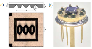
Pressure sensor chip utilizing electrical circuit of piezosensitive differential amplifier with negative feedback loop (PDA-NFL) for 5 kPa
XI International Scientific and Technical Conference 
"Micro-, and Nanotechnology in Electronics", 
Elbrus, Russia; June 2021
  
Dukhov Automatics Research Institute VNIIA, Moscow

Abstract: High sensitive (S=11.2±1.8 mV/V/kPa with nonlinearity error 2KNL=0.15±0.09 % /FS) small-sized (4.00x4.00 mm2) silicon pressure sensor chip utilizing new electrical circuit for microelectromechanical systems (MEMS) in the form of differential amplifier with negative feedback loop (PDA-NFL) for 5 kPa differential was developed. The advantages are demonstrated in the array of output characteristics, which prove the relevance of the presented development, relative to modern developments of pressure sensors with Wheatstone bridge electrical circuit for 5 kPa range.

Fig: a) Pressure sensor chip, b) its assembled structure


Feb 2, 2022

[EZMod3D] Comparing inductance extraction to measurement

EZMod3D is a division of EASii IC, which develops a 3D multi-domain physical simulation software solution (also called 3D field solver) mainly developed to process the design of integrated circuits (ASICs), printed circuit boards (PCBs) and both at the same time (CoDesign). EZMod3D was developed on the basis of an innovative solver enabling a fast simulation. This technology has allowed intensive use internally at EASii IC, targeting the requirements of R&D project: reducing iterations between design and manufacturing.

Very simple, you just need to start with your input data
  • GDS2 file, OASIS database, LEF / DEF (ASIC) or Gerber (PCB) or DXF (Packaging)
  • Technological file or materials description
  • The position of the potentials or flows to be applied
  • In pre-sizing step, you can sketchup using advanced user intergrated matrial library
FIG: An inductor, its 3D EZMod3D simulation and LCR measurements. EZMod3D now extracts inductance values and shows good agreement with measurements.
Measured value is 477nH; close to the simulated 481nH)

[paper] Modeling of SIC VDMOS FET

Anirban Kar∗, Ahtisham Pampori∗, Noriyoshi Hashimoto† and Yogesh Singh Chauhan∗
A Charge-Based Silicon Carbide MOSFET Compact Model for Power Electronics Applications
2021 IEEE 8th Uttar Pradesh Section UPCON)
DOI: 10.1109/UPCON52273.2021.9667643

∗Department of Electrical Engineering, IIT Kanpur (IN)
†Keysight Technologies (J)

Abstract: This paper presents a charge-based compact model for Silicon Carbide (SiC) power MOSFETs, which captures the static characteristics of the device over a wide range of voltages and currents. The drift region resistance and charges in the channel have been formulated to calculate the drain current in a self-consistent manner. The proposed model has been validated against the measured transfer and output characteristics of a commercial 1.2kV power MOSFET (Infineon IMW120R045M1) with a maximum current rating of 52A.

Fig: a) Transfer characteristics of SiC MOSFET with Vd=1 to 20V
b) Transconductance of SiC MOSFET with Vd=1 to 20V 

Acknowledgement: This work was supported in part by the Swarna Jayanti Fellowship under Grant DST/SJF/ETA02/2017-18 and in part by the Department of Science and Technology through the FIST Scheme under Grant SR/FST/ETII-072/2016 and Keysight Technologies, USA. The measurement of the device was carried out at Keysight Technologies, Japan.


Feb 1, 2022

IEEE SSCS PICO Contestants Cross the Finish Line

by Boris Murmann
DOI:10.1109/MSSC.2021.3135176
Date of current version: 24 January 2022

Last summer 2021, the IEEE Solid-State Circuits Society (SSCS) launched its first open source chip design contest under the umbrella of its Platform for Integrated Circuit Design Outreach program (PICO). Beginning with 61 submissions, a volunteer jury selected 18 teams from nine countries to embark on a journey toward tapeout. Anyone interested in supporting future activities is encouraged to sign up at the Society’s volunteer web portal. Stay tuned for the 2022 edition of the SSCS PICO contest!
FIG: Layout views of the chips submitted for tape out

      TABLE: A Summary Oof Designs Submitted for TapeOut
FunctionTeamChip URL
15G bidirectional amplifierPakistan 3 (National University of Computer and Emerging Sciences)https://efabless.com/projects/560
2Wireless power transfer unitPakistan 2 (National University of Computer and Emerging Sciences)
3Variable precision fused multiply–add unitPakistan 1 (National University of Computer and Emerging Sciences)
4Oscillator-based LVDT readoutIndia 2 (Anna University)https://efabless.com/projects/474
5Temperature sensorIndia 1 (Anna University)
6GPS baseband engineIndia 3 (Anna University)
7Ultralow-power analog front end for bio signalsBrazil 2 (Universidade Federal de Santa Catarina)https://efabless.com/projects/476
8TIA for quantum photonics interfaceUSA 4 (University of Virginia)https://efabless.com/projects/470
9Bandgap referenceEgypt (Cairo University)https://efabless.com/projects/473
10Neural network for sleep apnea detectionUSA 2 (University of Missouri)
11Sonar processing unitChile (University of the Bío-Bío)https://efabless.com/projects/54

Jan 31, 2022

[Google Research] Releases Circuit Training, an Open-Source Framework for Automated Chip Floorplanning #semi https://t.co/BD4iXWv5aS


from Twitter https://twitter.com/wladek60

January 31, 2022 at 05:48PM
via IFTTT