

Sep 30, 2011
Nonvolatile Memory Standard CMOS Process
Sep 23, 2011
8th International Conference on Devices, Circuits and Systems (ICCDCS)

ICCDCS is an IEEE-EDS technically sponsored international conference biannually held since its first edition (Caracas, 1995) at different locations within the Caribbean basin. Over time this conference has acquired a prestigious position as the outstanding international IEEE conference dealing with Electron Devices and Circuits and Systems which takes place within the Latin American Region.
Its main objective is to serve as a significant meeting point and technical forum to initiate, renew and maintain direct personal relations aimed at sharing relevant technical know-how among Latin American and rest-of-the-world professionals involved in the disciplines that it covers. Industry, Universities and R&D Institutions are invited to participate. English is the official working language of the Conference, although Spanish and Portuguese are also freely used in informal communications.
Prospective authors are invited to submit contributions for oral presentations to be reviewed by the Technical Program Committee. They should deal with new results, relevant ideas or innovations that advance the state-of-the-art in the areas of the Technical Program. Topics may span from basic theory to industrial applications, research, development, design, technology and applications of electron devices, analysis, design, and practical implementation of circuits, and their application to power electronics, telecommunications and instrumentation.
Location:
The ICCDCS'12 will be held on Playa del Carmen, México, from March 14 through March 17, 2012
You can download the pdf version of the Call for Papers here.
[Internship] Modeling of GaN Power Transistors for IC Design
Internship framework: At the heart of the MINATEC innovation campus, Leti institute is one of the most important R&D laboratories in Europe in the field of microelectronics and nanotechnologies. Within the Alternative Energies and Atomic Energy Commission, CEA-Leti is developing GaN-based technologies and power devices for energy conversion in different industrial fields (energy management, automotive electronics, electric car). In order to design and simulate integrated circuits, it is mandatory to develop electro-thermal models of power transistors.
Work description:
The aim of the internship is to develop a specific model for GaN-based high electron mobility transistors (HEMTs). This wide bandgap semiconductor is one of the most promising for power electronics and is currently the subject of extensive research. This internship will take place in the Simulation and Modeling laboratory (LSM) of the Silicon Components Division (DCOS).
This internship is divided into four parts:- Understanding of physical phenomena (electrical, thermal) in power HEMT transistors and analysis of existing models
- TCAD numerical simulations of devices.
- Compact modeling of transistors starting from previous studies on silicon carbide (SiC) transistors.
- Depending on availability, static and pulsed measurements on GaN transistors and extraction of model parameters.
Direction/Département/Service/Laboratoire CEA-LETI – DRT/DCOS/SCME/LSM
Postal address
CEA/GRENOBLE, MINATEC Campus,
17 rue des Martyrs 38054 Grenoble CEDEX 9
France
Technical Supervisor
Patrick MARTIN
Phone: 04 38 78 67 05
Sep 22, 2011

Sep 20, 2011
Digging into Technology's Past
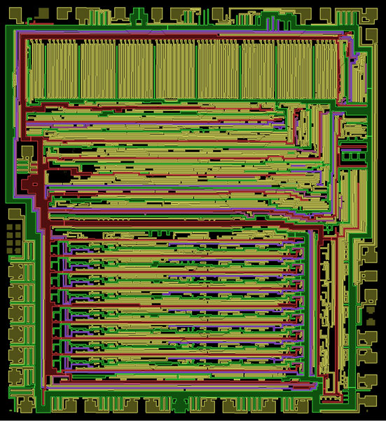
This detailed line drawing of the MOS Technology 6502 microprocessor is a physical description of all the connections between the various circuits on the chip. (Courtesy Greg James, Visual 6502, more in archaeology by Nikhil Swaminathan)
Sep 13, 2011
FAST-SPICE BETA TESTERS WANTED
All participants in the beta-testing program will receive the Symica Fast-SPICE product SymSpice Turbo as a free addition to the Symica tool suite. If you'd like to be a beta tester for the SymSpice Turbo, please send a request to support@symica.com. [more at: http://www.symica.com/news/fast-spice-beta-testers-wanted]
Sep 9, 2011

Sep 2, 2011
“The Ugly Duckling,” New Fairy Tales
"The developments of UF process-based “compact” MOSFET models have been reviewed, and exemplary new physical insights on SOI devices attained with the models have been overviewed. Indeed, the UF models have been, and are effective research/education tools. The “ugly duckling” has prevailed, just like in the fairy tale (illustrated in Fig. 10) [19]!" J. G. Fossum

[19] H. C. Anderson, “The Ugly Duckling,” New Fairy Tales. C. A. Reitzel, Copenhagen, Denmark, Nov. 1843.
in
J. Fossum, “UF ‘ Compact ’ Models : A Historical Perspective,” Nanotech, vol. 2, pp. 714 - 719, 2011.
Aug 31, 2011
Operation and Modeling of the MOS Transistor
Yannis Tsividis and Colin McAndrew
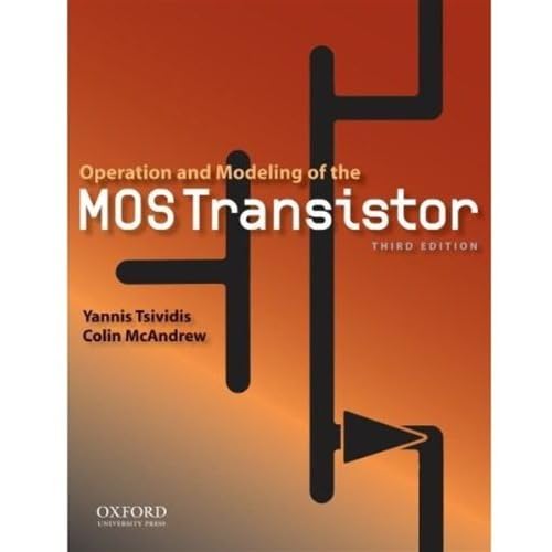
New to this edition:
ISBN-10: 0195170156 | ISBN-13: 978-0195170153 | Edition: 3
New to this edition:
- Energy bands and the energy barrier viewpoint are integrated into the discussion in a smooth, simple manner
- Expanded discussion of small-dimension effects, including velocity saturation, drain-induced barrier lowering, ballistic operation, polysilicon depletion, quantum effects, gate tunneling current, and gate-induced drain leakage
- Expanded discussion of small-signal modeling, including gate and substrate current modeling and flicker noise
- New chapter on substrate nonuniformity and structural effects, discussing transversal and lateral (halo) doping nonuniformity, stress and well proximity effects, and statistical variability
- A completely re-written chapter on modeling for circuit simulation, covering the considerations and pitfalls in the development of models for computer-aided design
- Extensively updated bibliography
- An accompanying website includes additional details not covered in the text, as well as model computer code
Jul 24, 2011
[mos-ak] Final Program MOS-AK/GSA ESSDERC/ESSCIRC Workshop in Helsinki on Sept.16 2011
Please visit the MOS-AK/GSA Helsinki web site with the final workshop
program:
http://www.mos-ak.org/helsinki/
program:
http://www.mos-ak.org/helsinki/
* Free On-line Registration Form:
http://essderc2011.org/registration_form.php
* Venue: Finlandia Hall in Helsinki, Finland
http://www.essderc2011.org/venue.php
* Agenda: Sept. 16, 2011: 8:30 - 16:30
http://www.mos-ak.org/helsinki/
With panel discussion: "40th Anniversary of SPICE"
(panelists alphabetic list)
Narain D. Arora, Siltera, USA
Christian Enz, EPFL, CH
Chenming Hu, UC Berkeley, USA
Willy Sansen, ESAT-MICAS, B (moderator)
Andrei Vladimirescu, BWRC, UC Berkeley, USA
Andreas Wild, ENIAC - JU, EU
--
You received this message because you are subscribed to the Google Groups "mos-ak" group.
To post to this group, send email to mos-ak@googlegroups.com.
To unsubscribe from this group, send email to mos-ak+unsubscribe@googlegroups.com.
For more options, visit this group at http://groups.google.com/group/mos-ak?hl=en.
Jul 18, 2011
Post Doctoral Researcher / Research Engineer Position in Compact Modeling
The BSIM Group of Electrical Engineering Department at the University of California Berkeley is seeking to hire a bright candidate interested in compact model development/maintenance to join as a post doctoral researcher or research engineer. We are looking for a candidate with PhD (for post doctoral researcher) or Masters (for Research Engineer) degree in EE/Physics preferably for long term (4–5 years). The responsibilities include but not limited to
- Research and development of new BSIM compact models
- Maintenance and support of BSIM MOSFET compact models (BSIM4, BSIMSOI and BSIM-MG)
- Interface with industry to understand requirements and issues with BSIM models and rectify them
- C & Verilog-A coding and testing/debugging of models
- Excellent semiconductor device physics and process technology knowledge
- Experience in computer programming (C and Verilog-A)
- Knowledge of basic analog and digital circuit operation
For more information, please visit:
BSIM Group and Device Group
Jun 29, 2011
Arrays of indefinitely long uniform nanowires and nanotubes
Arrays of indefinitely long uniform nanowires and nanotubes
- Nature Materials 10, 494–501 (2011)
- doi:10.1038/nmat3038
http://www.nature.com/nmat/journal/v10/n7/full/nmat3038.html
It's frankly nice.... see one of their pictures (hope they don't get too upset!):

Jun 23, 2011
SISPAD 2011 Companion Workshops
September 7, 2011; Hotel Hankyu Expo Park, Osaka, Japan
- Compact Modeling
- Organizer: Sadayuki Yoshitomi, Toshiba Corporation
- Power Devices
- Organizer: Ichiro Omura, Kyusyu Institute of Technology
[link]
SuVolta creates new transistor option for 20 nm
SuVolta creates new transistor option for 20 nm: "SuVolta, a startup process IP company with deep roots indevice design and m..."
Jun 22, 2011
Job offers at RF Micro Devices (RFMD)
I've seen that there are three job offers for Compact Modeling engineers at RFMD:
Tracking Code Job Title Location Date Posted
Note that this is only a re-diffusion of some information we've got, and that we're not related to them in any way!
Tracking Code Job Title Location Date Posted
| 12134 | Senior Modeling Engineer | Greensboro, NC, US | 6/7/2011 |
| 12117 | Sr. TCAD Modeling Engineer | Greensboro, NC, US | 5/26/2011 |
| 12116 | Sr. Modeling Engineer | Greensboro, NC, US | 5/24/2011 |
Note that this is only a re-diffusion of some information we've got, and that we're not related to them in any way!
Jun 17, 2011
Get your own version of Myfab LIMS

Myfab is the Swedish national research infrastructrue for micro and nano fabrication. Use the best cleanroom facilities in Sweden through our laboratory network and bring new scope and opportunity to your research and technical development. [read more]
IMEC benchmarks FinFET superiority
IMEC benchmarks FinFET superiority:
LONDON - The IMEC research institute has compared one planar and two FinFET technologies to see how they perform against scaling and process variability.
The benchmark circuits were six-transistor SRAM cells and SRAM arrays and IMEC has concluded that the FinFET outperforms planar CMOS in variability-aware and technology-aware comparison of SRAM product yield.
Both FinFET on bulk and FinFET on silicon-on-insulaor (SOIFF) technologies come out superior to the planar technology for medium- to large-sized SRAM arrays resulting in higher yields, IMEC said, although it did not disclose the process geometry at which the tests were done. It is likely to have been at around 28 to 22 nm.
As the dimensions of devices scale down, the variations in the electrical parameters of CMOS transistors steadily increase. This is due to random fluctuations in the density of the dopants in the channel, source, and drain. So, two closely placed transistors that are supposedly identical can show a widely different behavior. This makes the design of SRAM memory cells less predictable and controllable for every new technology node.
Because of this scaling 6T planar SRAMs below 22 nm remains challenging, IMEC said. FinFET devices show a lower leakage and variability and it is possible to design more compact cells.
Both FinFET technologies come out as superior to planar for SRAM arrays of greater than 128 kbytes. They are less sensitive to mismatches, thus allowing a more aggressive scaling of the power supply and a lower VCC than planar arrays. For undoped silicon-on-insulator FinFETs (SOIFF), the power supply can be lowered by an additional 200-mV compared to planar. As a sample result: undoped SOIFF FinFET allow for a 95% yield at 0.7-V in 32-Mbit SRAM arrays, moving to Gbit arrays for higher voltages.
By Peter Clarke, EE Times -- EDN, June 16, 2011
The benchmark circuits were six-transistor SRAM cells and SRAM arrays and IMEC has concluded that the FinFET outperforms planar CMOS in variability-aware and technology-aware comparison of SRAM product yield.
Both FinFET on bulk and FinFET on silicon-on-insulaor (SOIFF) technologies come out superior to the planar technology for medium- to large-sized SRAM arrays resulting in higher yields, IMEC said, although it did not disclose the process geometry at which the tests were done. It is likely to have been at around 28 to 22 nm.
As the dimensions of devices scale down, the variations in the electrical parameters of CMOS transistors steadily increase. This is due to random fluctuations in the density of the dopants in the channel, source, and drain. So, two closely placed transistors that are supposedly identical can show a widely different behavior. This makes the design of SRAM memory cells less predictable and controllable for every new technology node.
Because of this scaling 6T planar SRAMs below 22 nm remains challenging, IMEC said. FinFET devices show a lower leakage and variability and it is possible to design more compact cells.
Both FinFET technologies come out as superior to planar for SRAM arrays of greater than 128 kbytes. They are less sensitive to mismatches, thus allowing a more aggressive scaling of the power supply and a lower VCC than planar arrays. For undoped silicon-on-insulator FinFETs (SOIFF), the power supply can be lowered by an additional 200-mV compared to planar. As a sample result: undoped SOIFF FinFET allow for a 95% yield at 0.7-V in 32-Mbit SRAM arrays, moving to Gbit arrays for higher voltages.
Jun 15, 2011
A new birth in the IEEE journals world...
Let's welcome them!
They are starting with some interesting papers on low-power and analog design with nanometer-scale variations.... Let's hope they go on...
IEEE Journal of Emerging and Selected Topics in Circuits and Systems (JETCAS)

We are honored to welcome readers and authors to the inaugural issue of the IEEE Journal on Emerging and Selected Topics in Circuits and Systems (JETCAS for short), which is sponsored by the IEEE Circuits and Systems Society (CAS-S.)

The journal, which is freely accessible on-line to all CAS-S members, aims to build a platform for the broad and timely dissemination of key innovative results and findings in rapidly-growing and/or emerging topic areas within the scope of the IEEE Circuits and Systems Society. Such potentially interdisciplinary emerging topics will be selected as long as, first, they are clearly situated at the forefront of current scientific and technological developments and, second, they are expected to grow over time in scientific and professional importance and, therefore, in the number of active practitioners. From this point of view, JETCAS is expected to create new communities interested in the long-term development of the most promising subjects presented in the journal. The editorial strategy followed by JETCAS will be the publication of Special Issues on the selected topics. These issues will include research contributions from leading experts and presentations geared towards a wide audience of scientists and pra

MASSOUD PEDRAM, Editor-in-Chief (EiC)

MANUEL DELGADO-RESTITUTO, Deputy EiC

ENRICO MACII, 2010-2011 VP Publications, IEEE CAS-S

GIANLUCA SETTI, 2010 President, IEEE CAS-S


Volume 1, Issue 1 - Inaugural Edition
http://ieeexplore.ieee.org/xpl/RecentIssue.jsp?punumber=5503868

Pedram, M.;  Delgado-Restituto, M.;  Macii, E.;  Setti, G., Inaugural Editorial
http://ieeexplore.ieee.org/stamp/stamp.jsp?tp=&arnumber=5765455

-----------------------------------------------------------------------------------------------------
Variation-Aware Design for Nanoscale VLSI Circuits and Systems
The focus of this issue is on the challenges faced in designing digital and analog circuits in nanoscale technologies, where variations due to process, environmental, and aging variations are substantial.  The root causes of these effects can generally be traced to scaling: with the drive towards even greater miniaturization, these problems become even more acute and it is imperative that they be addressed.  The solutions involve the invention of improved design techniques, better design automation, and closer interactions between the phenomenological root causes and the designer.  The six papers in this issue attempt to provide a view of the landscape, reflecting the current state of the art and future directions.

Sapatnekar, S. S., Guest Editorial
http://ieeexplore.ieee.org/stamp/stamp.jsp?tp=&arnumber=5762378

------------------------------------------------------------------------------------------------------------------
Sapatnekar, S. S., Overcoming Variations in Nanometer-Scale Technologies
http://ieeexplore.ieee.org/stamp/stamp.jsp?tp=&arnumber=5762377
Nanometer-scale circuits are fundamentally different from those built in their predecessor technologies in that they are subject to a wide range of new effects that induce on-chip variations. These include effects associated with printing finer geometry features, increased atomic-scale effects, and increased on-chip power densities, and are manifested as variations in process and environmental parameters and as circuit aging effects. The impact of such variations on key circuit performance metrics is quite significant, resulting in parametric variations in the timing and power, and potentially catastrophic failure due to reliability and aging effects. Such problems have led to a revolution in the way that chips are designed in the presence of such uncertainties, both in terms of performance analysis and optimization. This paper presents an overview of the root causes of these variations and approaches for overcoming their effects.
-----------------------------------------------------------------------------------------------------------------
Karakonstantis, G.;  Chatterjee, A.;  Roy, K., Containing the Nanometer "Pandora-Box": Cross-Layer Design Techniques for Variation Aware Low Power Systems
http://ieeexplore.ieee.org/stamp/stamp.jsp?tp=&arnumber=5766061
The demand for richer multimedia services, multifunctional portable devices and high data rates can only been visioned due to the improvement in semiconductor technology. Unfortunately, sub-90 nm process nodes uncover the nanometer Pandora-box exposing the barriers of technology scaling-parameter variations, that threaten the correct operation of circuits, and increased energy consumption, that limits the operational lifetime of today's systems. The contradictory design requirements for low-power and system robustness, is one of the most challenging design problems of today. The design efforts are further complicated due to the heterogeneous types of designs (logic, memory, mixed-signal) that are included in today's complex systems and are characterized by different design requirements. This paper presents an overview of techniques at various levels of design abstraction that lead to low power and variation aware logic, memory and mixed-signal circuits and can potentially assist in meeting the strict power b
-----------------------------------------------------------------------------------------------------------------
Mitra, S.;  Brelsford, K.;  Kim, Y. M.;  Lee, H.-H. K.;  Li, Y., Robust System Design to Overcome CMOS Reliability Challenges
http://ieeexplore.ieee.org/stamp/stamp.jsp?tp=&arnumber=5751208
Today's mainstream electronic systems typically assume that transistors and interconnects operate correctly over their useful lifetime. With enormous complexity and significantly increased vulnerability to failures compared to the past, future system designs cannot rely on such assumptions. For coming generations of silicon technologies, several causes of hardware reliability failures, largely benign in the past, are becoming significant at the system level. Robust system design is essential to ensure that future systems perform correctly despite rising complexity and increasing disturbances. This paper describes three techniques that can enable a sea change in robust system design through cost-effective tolerance and prediction of failures in hardware during system operation: 1) efficient soft error resilience; 2) circuit failure prediction; and 3) effective on-line self-test and diagnostics. The need for global optimization across multiple abstraction layers is also demonstrated.
-----------------------------------------------------------------------------------------------------------------
Seok, M.;  Chen, G.;  Hanson, S.;  Wieckowski, M.;  Blaauw, D.;  Sylvester, D., CAS-FEST 2010: Mitigating Variability in Near-Threshold Computing
http://ieeexplore.ieee.org/stamp/stamp.jsp?tp=&arnumber=5762379
Near threshold computing has recently gained significant interest due to its potential to address the prohibitive increase of power consumption in a wide spectrum of modern VLSI circuits. This tutorial paper starts by reviewing the benefits and challenges of near threshold computing. We focus on the challenge of variability and discuss circuit and architecture solutions tailored to three different circuit fabrics: logic, memory, and clock distribution. Soft-edge clocking, body-biasing, mismatch-tolerant memories, asynchronous operation and low-skew clock networks are presented to mitigate variability in the near threshold ${V} _{rm DD}$ regime.
-----------------------------------------------------------------------------------------------------------------
Maricau, E.;  Gielen, G., Computer-Aided Analog Circuit Design for Reliability in Nanometer CMOS
http://ieeexplore.ieee.org/stamp/stamp.jsp?tp=&arnumber=5762376
Integrated analog circuit design in nanometer CMOS technologies brings forth new and significant reliability challenges. Ever-increasing process variability effects and transistor wear-out phenomena such as BTI, hot carrier degradation and dielectric breakdown force designers to use large design margins and to increase the uncertainty on the circuit lifetime. To help designers to tackle these problems at design time (i.e., Design For Reliability, or DFR), accurate transistor aging models, efficient circuit reliability analysis methods and novel design techniques are needed. The paper overviews the current state of the art in DFR for analog circuits. The most important unreliability effects in nanometer CMOS technologies are reviewed and transistor aging models, intended for accurate circuit simulation, are described. Also, efficient methods for circuit reliability simulation and analysis are discussed. These methods can help designers to analyze their circuits and to identify weak spots. Finally, cost-effect
-----------------------------------------------------------------------------------------------------------------
Zhang, X.;  Mukadam, M. Y.;  Mukhopadhyay, I.;  Apsel, A. B., Process Compensation Loops for High Speed Ring Oscillators in Sub-Micron CMOS
http://ieeexplore.ieee.org/stamp/stamp.jsp?tp=&arnumber=5756255
In this paper, we present two implementations of a closed-loop process compensation scheme for high speed ring oscillators-the comparator based and the switched capacitor based loops. We provide detailed discussion of the frequency accuracy, loop stability, and implementation cost for each design. More than 150 test chips from multiple wafer-runs in a 90 nm CMOS process verify that frequency accuracy of better than 2.6% can be achieved with the application of the proposed compensation loop. Moreover, by leveraging a low variation addition-based current source, we have demonstrated a fully-integrated 2.15 GHz ring oscillator with less than 4.6% frequency variation without external references or post fabrication calibration, which is 3.8 $times$ improvement in frequency accuracy over the baseline case. The same compensation scheme can also alleviate frequency drift caused by temperature.

JETCAS is published quarterly and solicits, with particular emphasis on emerging areas, special issues on topics that cover the entire scope of the IEEE Circuits and Systems (CAS) Society, namely the theory, analysis, modeling, design, automation, and implementation of electronic circuits and systems, spanning theoretical foundations, applications, and architectures for signal and information processing.
Jun 13, 2011
First Graphene Integrated Circuit

IBM researchers have built the first IC based on a graphene transistor. It is another step toward overcoming the limits of silicon and a potential path to flexible electronics [read more at spectrum.ieee.org]
Jun 10, 2011
Alternative semiconductor fabrication methods enable inexpensive, conformable consumer devices - Solid State Technology
Alternative semiconductor fabrication methods enable inexpensive, conformable consumer devices - Solid State Technology
Emerging technology and a developing infrastructure for printed electronics is enabling circuitry that is flexible, conformable, and inexpensive to mass-produce. FlexTech Alliance has identified, funded, and directed advanced development in the flexible and printed electronics infrastructure, paving the way for the practical manufacture of a variety of low-cost applications such as electronic packaging, ID tags, and wide-area lighting panels.
Printed electronics include a set of consumer markets where printed logic and memory will be required. The size and cost of fully printed systems is set to challenge silicon-based technologies in ultra-high-volume distributed applications. To address this issue, Norwegian firm ThinFilm Electronics produces rewritable memory tags manufactured using full roll-to-roll (R2R) printing. Printed non-volatile RAM (NVRAM), when combined with printed transistor elements, serves as the basis of a new generation of cheap, disposable, and highly ubiquitous electronic devices. The company is working with major toy and game companies and has established high-volume manufacturing to deliver millions of tags per month.
In other commercial development, a new method for fabricating printed semiconductors, developed by NthDegree Technologies, allows a standard high-speed printing press to print conductive ink on to paper, plastic, or other substrate materials. Printed semiconductors made with these inks reduce the cost of producing semiconductor-based devices while creating innovative conformable products. Wide-area lighting is currently being produced with this technology by means of a light-emitting diode (LED) "ink". This LED ink is being used to print area lighting that is converted into a flat panel to replace fluorescent tube fixtures.
These latest developments in printed electronics materials, tools and processes, including LED lighting and printed memory, will be discussed and demonstrated at the Extreme Electronics TechXpot session "Printed electronics: Beyond R&D to real-deal technologies," presented by the FlexTech Alliance at SEMICON West, July 14, 2011. For more information about FlexTech Alliance visit www.flextech.org.
Freescale's Su calls for improved EDA tools
Freescale's Su calls for improved EDA tools:
As more embedded devices are being connected to the "Internet of things" the design methodologies used in IC designs need to change accordingly for faster chip turnarounds.

Su delivered the Tuesday (June 7) keynote here at the Design Automation Conference, whose organizers have placed embedded systems and software squarely in the apex of DAC with dedicated exhibit areas on the show floor.
While only 15 exhibitors specifically identified themselves as embedded hardware/software providers out of a total of 200, the technical program was loaded with embedded presentations and Su's keynote was clearly aimed at showing that at least Freescale understands that it is operating in a new space for them, the embedded world.
"The embedded era is defined by standards-based hardware and software, is open source, and aimed numerous markets, including health, safety, energy, transportation, communications, entertainment, automation, and, of course, cloud computing," said Su.
Su quoted statistics that the monthly mobile traffic will increase tenfold from today's 0.6 exabytes to 6.3 exabytes by 2015. "The resultant heterogeneous networks, together with the increasing needs of the ‘connected' car, offer many opportunities to semiconductor companies like us," said Su.
The many-core paradigm of the expected SOC technology transition poses a few challenges, according to Su.
Among these are scalability as the number of cores per processor generation will double. Also there will be system tradeoffs to consider between cores versus using hardware acceleration, as well cluster optimization among cores, caches, local vs. global resource sharing. And an increasing amount of high-speed mixed-signal I/O will place strain on expected quality of service metrics.
read more...
As more embedded devices are being connected to the "Internet of things" the design methodologies used in IC designs need to change accordingly for faster chip turnarounds.
Lisa Su, VP and general manager of Freescale"Some 7 billion devices will be connected to the Internet in this era from 2006 to 2020," said Lisa Su, vice president and general manager of Freescale Semiconductor Inc's networking and multimedia group. "And mobile traffic is doubling every year through 2015."
Su delivered the Tuesday (June 7) keynote here at the Design Automation Conference, whose organizers have placed embedded systems and software squarely in the apex of DAC with dedicated exhibit areas on the show floor.
While only 15 exhibitors specifically identified themselves as embedded hardware/software providers out of a total of 200, the technical program was loaded with embedded presentations and Su's keynote was clearly aimed at showing that at least Freescale understands that it is operating in a new space for them, the embedded world.
"The embedded era is defined by standards-based hardware and software, is open source, and aimed numerous markets, including health, safety, energy, transportation, communications, entertainment, automation, and, of course, cloud computing," said Su.
Su quoted statistics that the monthly mobile traffic will increase tenfold from today's 0.6 exabytes to 6.3 exabytes by 2015. "The resultant heterogeneous networks, together with the increasing needs of the ‘connected' car, offer many opportunities to semiconductor companies like us," said Su.
The many-core paradigm of the expected SOC technology transition poses a few challenges, according to Su.
Among these are scalability as the number of cores per processor generation will double. Also there will be system tradeoffs to consider between cores versus using hardware acceleration, as well cluster optimization among cores, caches, local vs. global resource sharing. And an increasing amount of high-speed mixed-signal I/O will place strain on expected quality of service metrics.
read more...
Jun 8, 2011
Postdoc Position in Thin Films (Thun, CH)
Empa is the interdisciplinary research and services institution for material sciences and technology development of the ETH Domain. Laboratory for Mechanics of Materials and Nanostructures at Empa's location in Thun, CH, is offering an Academia / Industry Postdoc Position in Thin Films
Submit your application online and upload all documents through this webpage by June 30, 2011:
http://internet1.refline.ch/673276/0190/++publications++/1/index.html
Additional information can be obtained from the EMPA website and by contacting Dr. Johann Michler.
Submit your application online and upload all documents through this webpage by June 30, 2011:
http://internet1.refline.ch/673276/0190/++publications++/1/index.html
Additional information can be obtained from the EMPA website and by contacting Dr. Johann Michler.
IEDM'2011 Abstract Submission Site is Now Open (Deadline: June 24, 2011)
IEDM Abstract Submission Site is Now Open - Abstract Submission
Deadline:   June 24, 2011

2011 IEEE International Electron Devices Meeting
The Annual Technical Meeting of the Electron Devices Society will be held at the
Washington Hilton, Washington, DC USA  - December 5-7, 2011

To view the IEDM Call for Papers and instructions for submitting an abstract to
the conference, visit:      http://www.ieee-iedm.org

IEEE International Electron Devices Meeting (IEDM) is the world’s pre-eminent
forum for reporting technological breakthroughs in the areas of semiconductor
and electronic device technology, design, manufacturing, physics, and modeling.
IEDM is the flagship conference for nanometer-scale CMOS transistor technology,
advanced memory, displays, sensors, MEMS devices, novel quantum and nano-scale
devices and phenomenology, optoelectronics, devices for power and energy
harvesting, high-speed devices, as well as process technology and device
modeling and simulation.

Starting this year (2011) there is an increased emphasis on circuit and device
interaction.  With ever increasing transistor count, nanometer design rules and
layout restrictions, circuit-device interaction is becoming critical to
providing viable technology solutions. This new emphasis includes
technology/circuit co-optimization, power/performance/area analyses, design for
manufacturing and process control, as well as CMOS platform technology and
scaling.

INCREASED PARTICIPATION IN THE FOLLOWING AREAS IS SOUGHT:
 * Circuit-device interaction
 * Energy harvesting
 * Biomedical devices
 * Power devices

Information about IEDM can be found at: http://www.ieee-iedm.org
Twitter: http://twitter.com/ieee_iedm
Facebook: http://www.facebook.com/pages/IEDM/131119756449

MEETING HIGHLIGHTS
 * New subcommittees (Circuit-Device Interaction and Nano Device Technology)
 * New for 2011:  90 Minute Tutorial Sessions on Emerging Topics, Saturday
afternoon, December 3
 * Three plenary presentations by prominent experts
 * Invited papers on all aspects of advanced devices and technologies.
 * An Emerging Technology session.
 * Two evening Panel discussions.
 * Presentation of IEEE/EDS awards.
 * IEDM Luncheon presentation will be held on Tuesday, December 6.
 * Two short courses will be held on Sunday, December 4.

Further Information - All questions or inquiries for further information
regarding this meeting should be directed to the Conference Office at:

19803 Laurel Valley Place
Montgomery Village, MD 20886 USA
Tel: 301-527-0900, ext. 2
Email: iedm@his.com
Local European Contact

Stefan De Gendt, IMEC, Belgium
Local Asian Contact
Norikatsu Takaura, LEAP, Japan
2011 Conference Chair
Kazunari Ishimaru, Toshiba, Japan
Technical Program Chair
Veena Misra, North Carolina State University, USA

If you know of any colleagues who may have a paper to contribute and have not
received this notice, please bring it to their attention.
Jun 3, 2011
Course on Statistical CMOS Variability and Reliability, San Jose CA, June 13th and 14th
Professor Asen Asenov, CEO of Gold Standard Simulations, will be delivering a comprehensive course (see the flyer) on variability and reliability issues and their impact on modern CMOS devices and design.
The course topics include, Variability classification,Sources of statistical variability, Simulation of statistical variability, Variability trends in conventional and novel MOSFETs, Random telegraph noise statistics, Statistical aspects of reliability, Statistical compact model strategies and Statistical circuit simulation. At this event there will also be a special lecture on Variability in FinFET devices.
For more information please visit: http://www.goldstandardsimulations.com/courses/ or get in touch with them at courses(at)goldstandardsimulations.com.
Jun 2, 2011
Papers in Solid-State Electronics Volume 62, Issue 1, (August 2011)
A computationally efficient compact model for fully-depleted SOI MOSFETs with independently-controlled front- and back-gates Original Research Article
Pages 31-39
Darsen D. Lu, Mohan V. Dunga, Chung-Hsun Lin, Ali M. Niknejad, Chenming Hu
An effective thermal circuit model for electro-thermal simulation of SOI analog circuits Original Research Article
Pages 48-61
Ming-C. Cheng, Kun Zhang
MOSFET modeling for design of ultra-high performance infrared CMOS imagers working at cryogenic temperatures: Case of an analog/digital 0.18 μm CMOS process Original Research Article
Pages 115-122
P. Martin, A.S. Royet, F. Guellec, G. Ghibaudo
Physics-based compact model for ultra-scaled FinFETs Original Research Article
Pages 165-173
Ashkhen Yesayan, Fabien Prégaldiny, Nicolas Chevillon, Christophe Lallement, Jean-Michel Sallese
Three-dimensional analytic modelling of front and back gate threshold voltages for small geometry fully depleted SOI MOSFET’s Original Research Article
Pages 174-184
Krishna Meel, R. Gopal, Deepak Bhatnagar
Mobility analysis of surface roughness scattering in FinFET devices Original Research Article
Pages 195-201
Jae Woo Lee, Doyoung Jang, Mireille Mouis, Gyu Tae Kim, Thomas Chiarella, Thomas Hoffmann, Gérard Ghibaudo
Pages 31-39
Darsen D. Lu, Mohan V. Dunga, Chung-Hsun Lin, Ali M. Niknejad, Chenming Hu
Research highlights
► A computationally efficient approximation for surface potential in FDSOI MOSFETs is developed. ► I–V and C–V models for FDSOI MOSFETs are derived without making the charge sheet approximation. ► The core model and non-ideal effect expressions are implemented in Verilog-A language. ► The model is symmetric with respect to Vds = 0 and continuous in all regions of operation.An effective thermal circuit model for electro-thermal simulation of SOI analog circuits Original Research Article
Pages 48-61
Ming-C. Cheng, Kun Zhang
Highlights
► A thermal circuit model is developed for SOI analog circuits. ► The model integrates a device thermal circuit with interconnect thermal networks. ► The device thermal circuit accounts for non-isothermal effects in SOI devices. ► Thermal networks for cross-coupled and parallel coupled wires are developed. ► The model is coupled with BSIMSOI for electro-thermal simulation of SOI circuits.MOSFET modeling for design of ultra-high performance infrared CMOS imagers working at cryogenic temperatures: Case of an analog/digital 0.18 μm CMOS process Original Research Article
Pages 115-122
P. Martin, A.S. Royet, F. Guellec, G. Ghibaudo
Research highlights
► Specific physical effects are observed in a cooled (77–200 K) 0.18 μm CMOS process. ► These effects are described and modeled for design of cryogenic IR CMOS imagers. ► Data on low frequency noise and transistor matching in MOSFET are also presented.Physics-based compact model for ultra-scaled FinFETs Original Research Article
Pages 165-173
Ashkhen Yesayan, Fabien Prégaldiny, Nicolas Chevillon, Christophe Lallement, Jean-Michel Sallese
Highlights
► We propose a physical and explicit compact model for lightly doped FinFETs. ► This design-oriented model is valid for a large range of silicon Fin widths/lengths. ► It describes well the drain current, small signal parameters and capacitances. ► It takes into account all short-channel effects and quantum mechanical effects. ► This compact model needs a very few number of electrical parameters (4).Three-dimensional analytic modelling of front and back gate threshold voltages for small geometry fully depleted SOI MOSFET’s Original Research Article
Pages 174-184
Krishna Meel, R. Gopal, Deepak Bhatnagar
Highlights
► New 3-D front (back) gate threshold voltage models of FD-SOI MOSFETs are reported. ► Models solve 3-D Poisson’s equation using Green’s function as a tool. ► 3-D threshold voltage models include side wall, source/drain and back gate effects. ► Front and back gate charge coupling is incorporated in both the threshold voltages. ► Compact models of threshold voltages are amenable to circuit CAD tool.Mobility analysis of surface roughness scattering in FinFET devices Original Research Article
Pages 195-201
Jae Woo Lee, Doyoung Jang, Mireille Mouis, Gyu Tae Kim, Thomas Chiarella, Thomas Hoffmann, Gérard Ghibaudo
Highlights
► Mobility analysis of the surface roughness scattering along the different interfaces of FinFET devices. ► The sidewall and top surface drain current components were estimated from the total drain currents of different fin width conditions. ► The contribution of the surface roughness scattering was analysed and that on sidewalls was about three times stronger than on top surface for n-channel FinFETs.Jun 1, 2011
[mos-ak] C4P MOS-AK/GSA ESSDERC/ESSCIRC Workshop in Helsinki on Sept.16 2011
C4P MOS-AK/GSA ESSDERC/ESSCIRC Workshop in Helsinki on Sept.16 2011
http://www.mos-ak.org/helsinki/
http://www.mos-ak.org/helsinki/
Together with the Organizing Committee and Extended MOS-AK/GSA TPC
Committee, we have pleasure to invite to the MOS-AK/GSA Workshop in
Helsinki on Sept.16 2011 with special panel: 40th Anniversary of SPICE
(panelists tentative alphabetic list):
* Narain D. Arora, Siltera, USA
* Christian Enz, CSEM, CH
* Andrei Vladimirescu, EECS, Berkeley
* Andreas Wild, ENIAC - JU, EU
and MOS-AK/GSA Transistor Level IC Design Challenge Opening
The MOS-AK/GSA Workshop is HiTech forum to discuss the frontiers of
the electron devices modeling with emphasis on simulation-aware
models. Original papers presenting new developments and advances in
the compact/spice modeling and its Verilog-A standardization are
solicited. The main topics of the workshop are: (but are not limited
to):
* Compact Modeling (CM) of the electron devices
* VHDL-AMS/Verilog-A for CM standardization
* New CM techniques and extraction software
* CM of passive, active, sensors and actuators
* Emerging devices, CMOS and SOI-based memory cells
* Microwave, RF device modeling, high voltage device modeling
* Transistor Level IC support
* Nanoscale CMOS devices and circuits
* Reliability and thermal management of electron devices
* Technology R&D, DFY, DFT and IC designs
* Foundry/Fabless interface strategies
The terms of participation:
Authors are asked to submit a short (~200words) abstract using on-line
submission form by JUNE 30 http://www.mos-ak.org/helsinki/abstracts.php
Intending authors should also note the following deadlines:
* Announcement and Call for Papers - May 2011
* on-line abstract submission deadline - June 30, 2011
* Final Workshop Program - August 2011
* MOS-AK/GSA Workshop - Sept. 16, 2011
On-line workshop registration: http://www.essderc2011.org/registration.php
Further details and updates: http://www.mos-ak.org/helsinki
Email contact: helsinki@mos-ak.org
--
You received this message because you are subscribed to the Google Groups "mos-ak" group.
To post to this group, send email to mos-ak@googlegroups.com.
To unsubscribe from this group, send email to mos-ak+unsubscribe@googlegroups.com.
For more options, visit this group at http://groups.google.com/group/mos-ak?hl=en.
May 25, 2011
Papers for curious people... (may 25th 2011)
CMOS Silicon Physical Unclonable Functions Based on Intrinsic Process Variability
Stanzione, S. Puntin, D. Iannaccone, G.Page(s): 1456 - 1463
Digital Object Identifier : 10.1109/JSSC.2011.2120650
AbstractPlus | Full Text: PDF (1209KB)
This paper presents an extreme-low-power mixed-signal CMOS integrated circuit for product identification and anti-counterfeiting, which implements a physical unclonable function operating with a challenge-response scheme. We devise a series of circuits and algorithmic solutions based on the use of a process monitor and on the prediction of the erratic response bits which allow to suppress the effects of temperature, voltage supply and process variations in order to obtain a robust and reliable b... Read More »
Page(s): 1284 - 1295
Digital Object Identifier : 10.1109/JSSC.2011.2120690
A Supply-Rail-Coupled eTextiles Transceiver for Body-Area Networks
Mercier, P. P. Chandrakasan, A. P.Page(s): 1284 - 1295
Digital Object Identifier : 10.1109/JSSC.2011.2120690
AbstractPlus | Full Text: PDF (1915KB)
This paper presents a transceiver that communicates over electronic textiles as an alternative, energy-efficient communication medium for body-area network (BAN) applications. The proposed eTextiles network architecture consists of a two-wire conductive yarn medium, body-worn nodes, and a basestation used for data collection and medium-access control. Fabricated in 0.18 $mu$m CMOS technology, the eTextiles transceiver employs supp... Read More »
Page(s): 987 - 996
Digital Object Identifier : 10.1109/TVLSI.2010.2043694
Page(s): 1094 - 1098
Digital Object Identifier : 10.1109/TVLSI.2010.2043695
Page(s): 1104 - 1108
Digital Object Identifier : 10.1109/TVLSI.2010.2044049
Statistical Modeling and Simulation of Threshold Variation Under Random Dopant Fluctuations and Line-Edge Roughness
Ye, Y. Liu, F. Chen, M. Nassif, S. Cao, Y.Page(s): 987 - 996
Digital Object Identifier : 10.1109/TVLSI.2010.2043694
The threshold voltage $({V}_{rm th})$ of a nanoscale transistor is severely affected by random dopant fluctuations and line-edge roughness. The analysis of these effects usually requires atomistic simulations which are too expensive in computation for statistical design. In this work, we develop an efficient SPICE simulation method and statistical variation model that accurately predict threshold variation as a function of dopant ... Read More »
On Functional Broadside Tests With Functional Propagation Conditions
Pomeranz, I. Reddy, S. M.Page(s): 1094 - 1098
Digital Object Identifier : 10.1109/TVLSI.2010.2043695
AbstractPlus | Full Text: PDF (197KB)
Functional broadside tests were defined as broadside tests where the scan-in state is a reachable state. This ensures that during the functional capture cycles of the test, the circuit visits states that it can also visit during functional operation. As a result, it avoids overtesting that may occur with unreachable states. However, the scan-out operation at the end of a functional broadside test allows the observation of any fault effects that reached the state variables at the end of the secon... Read More »
Broadside and Functional Broadside Tests for Partial-Scan Circuits
Pomeranz, I. Reddy, S. M.Page(s): 1104 - 1108
Digital Object Identifier : 10.1109/TVLSI.2010.2044049
AbstractPlus | Full Text: PDF (176KB)
Functional broadside tests were defined to address overtesting that may occur due to the detection of delay faults under nonfunctional operation conditions. Such conditions are made possible by scanning in unreachable states. Functional broadside tests were defined and studied in the context of full-scan circuits. In this work, we study the definition of broadside and functional broadside tests in partial-scan circuits. A unique property we show is that if the unscanned state variables are obser... Read More »
Papers in IEEE TED, vol 58, issue 6 (june 2011)
An Efficient Robust Algorithm for the Surface-Potential Calculation of Independent DG MOSFET
Jandhyala, S. Mahapatra, S.Page(s): 1663 - 1671
Digital Object Identifier : 10.1109/TED.2011.2131654
Although the recently proposed single-implicit-equation-based input voltage equations (IVEs) for the independent double-gate (IDG) MOSFET promise faster computation time than the earlier proposed coupled-equations-based IVEs, it is not clear how those equations could be solved inside a circuit simulator as the conventional Newton–Raphson (NR)-based root finding method will not always converge due to the presence of discontinuity at the G-zero point (GZP) and nonremovable singularities in ... Read More »
Page(s): 1672 - 1680
Digital Object Identifier : 10.1109/TED.2011.2131144
Statistical Model of Line-Edge and Line-Width Roughness for Device Variability Analysis
Hiraiwa, A. Nishida, A. Mogami, T.Page(s): 1672 - 1680
Digital Object Identifier : 10.1109/TED.2011.2131144
The authors propose a model of line-edge and line-width roughness (LER and LWR) of actual device patterns, which received some smoothing steps, for accurate estimation of device variability. The model assumes that LER/LWR has originally an exponential autocorrelation function (ACF) and is smoothed using another exponential function. The power spectrum of this ACF almost completely fits the experimental one of polycrystalline silicon lines, which were formed using plasma etching. The authors inve... Read More »
Page(s): 1710 - 1721
Digital Object Identifier : 10.1109/TED.2011.2119487
A Physics-Based Analytical Compact Model for the Drift Region of the HV-MOSFET
Bazigos, A. Krummenacher, F. Sallese, J.-M. Bucher, M. Seebacher, E. Posch, W. Moln??r, K. Tang, M.Page(s): 1710 - 1721
Digital Object Identifier : 10.1109/TED.2011.2119487
This paper presents a novel physics-based analytical compact model for the drift region of a high-voltage metal–oxide–semiconductor field-effect transistor (HV-MOSFET). According to this model, the drift region is considered as a simple 1-D problem, just as that of a low-voltage inner MOS transistor. It exploits the charge-sheet approximation and performs linearization between the charge in the drift region and the surface potential. The drift region model combined with the standar... Read More »
Papers in IEEE EDL, vol 32, issue 6 (may 2011)
Modeling of Current-Return-Path Effect on Single-Ended Inductor in Millimeter-Wave Regime
Wang, H. Zhang, L. Yang, D. Zeng, D. Wang, Y. Yu, Z.Page(s): 737 - 739
Digital Object Identifier : 10.1109/LED.2011.2136312
The effect of current return path (CRP) on the accurate modeling of single-ended inductors in the millimeter-wave regime has been investigated. A series of spiral inductors with different sizes, shapes, and CRP positions was fabricated in a 0.18-$muhbox{m}$ RF-CMOS process and measured up to 50 GHz. An analytical appended model for CRP is developed to characterize the effect, and its equivalent circuit is validated by measurement ... Read More »
Page(s): 704 - 706
Digital Object Identifier : 10.1109/LED.2011.2127441
Page(s): 722 - 724
Digital Object Identifier : 10.1109/LED.2011.2131116
Simple Analytical Bulk Current Model for Long-Channel Double-Gate Junctionless Transistors
Duarte, J. P. Choi, S.-J. Moon, D.-I. Choi, Y.-K.Page(s): 704 - 706
Digital Object Identifier : 10.1109/LED.2011.2127441
A bulk current model is formulated for long-channel double-gate junctionless (DGJL) transistors. Using a depletion approximation, an analytical expression is derived from the Poisson equation to find channel potential, which expresses the dependence of depletion width under an applied gate voltage. The depletion width equation is further simplified by the unique characteristic of junctionless transistors, i.e., a high channel doping concentration. From the depletion width formula, the bulk curre... Read More »
Modeling and Separate Extraction of Gate-Bias- and Channel-Length-Dependent Intrinsic and Extrinsic Source–Drain Resistances in MOSFETs
Bae, H. Jang, J. Shin, J. S. Yun, D. Lee, J. Kim, T. W. Kim, D. H. Kim, D. M.Page(s): 722 - 724
Digital Object Identifier : 10.1109/LED.2011.2131116
A new technique for a separate extraction of the current-path-dependent resistance $(R_{{rm SD}0})$ from the contact-dependent source and drain resistances $(R_{rm Se} hbox{and} R_{rm De})$ is reported for a single MOSFET. We also report a technique for a separation of $V_{rm GS}$ -dependent source an... Read More »
Extraction of Separated Source and Drain Resistances in Amorphous Indium–Gallium–Zinc Oxide TFTs Through
Bae, H. Kim, S. Bae, M. Shin, J. S. Kong, D. Jung, H. Jang, J. Lee, J. Kim, D. H. Kim, D. M.
Page(s): 761 - 763
Digital Object Identifier : 10.1109/LED.2011.2127438
Page(s): 764 - 766
Digital Object Identifier : 10.1109/LED.2011.2132112
Page(s): 773 - 775
Digital Object Identifier : 10.1109/LED.2011.2125940
Extraction of Separated Source and Drain Resistances in Amorphous Indium–Gallium–Zinc Oxide TFTs Through  –
–  Characterization
Bae, H. Kim, S. Bae, M. Shin, J. S. Kong, D. Jung, H. Jang, J. Lee, J. Kim, D. H. Kim, D. M. Page(s): 761 - 763
Digital Object Identifier : 10.1109/LED.2011.2127438
Considering asymmetry caused by layout, process, and device degradation, separate extraction of the source and drain resistances, i.e., $R_{S}$ and $R_{D}$, respectively, from the total resistance $R_{rm TOT}$ is very important in the design, modeling, and characterization of amorphous indium–g... Read More »
Mechanism Analysis of Off-Leakage Current in an LDD Poly-Si TFT Using Activation Energy
Nakashima, A. Kimura, M.Page(s): 764 - 766
Digital Object Identifier : 10.1109/LED.2011.2132112
We have analyzed the mechanism of off-leakage current in an lightly doped drain (LDD) poly-Si thin-film transistor by investigating the activation energy $E_{a}$. It is found that $E_{a}$ decreases as the gate and drain voltages increase. We have also discussed the mechanism using a device simulator. It is found that a hole channel is lightly formed in the LDD regio... Read More »
Evidence of a Novel Source of Random Telegraph Signal in CMOS Image Sensors
Goiffon, V. Magnan, P. Martin-Gonthier, P. Virmontois, C. Gaillardin, M.Page(s): 773 - 775
Digital Object Identifier : 10.1109/LED.2011.2125940
This letter reports a new source of dark current random telegraph signal in CMOS image sensors due to meta-stable Shockley–Read–Hall generation mechanism at oxide interfaces. The role of oxide defects is discriminated thanks to the use of ionizing radiations. A dedicated RTS detection technique and several test conditions (radiation dose, temperature, integration time, photodiode bias) reveal the particularities of this novel source of RTS. Read More »
Page(s): 791 - 793
Digital Object Identifier : 10.1109/LED.2011.2135835
Temperature Dependence of the Threshold Voltage Shift Induced by Carrier Injection in Integrated STI-Based LDMOS Transistors
Poli, S. Reggiani, S. Denison, M. Gnani, E. Gnudi, A. Baccarani, G. Pendharkar, S. Wise, R.Page(s): 791 - 793
Digital Object Identifier : 10.1109/LED.2011.2135835
Large threshold voltage shifts $(Delta V_{t})$ are experimentally observed in n-channel lateral DMOS transistors under high current–voltage regime. The effect is enhanced by the gate voltage as well as by the ambient temperature $(T_{A})$ . By approximating the curves with the usually adopted power-law dependence ... Read More »
Page(s): 809 - 811
Digital Object Identifier : 10.1109/LED.2011.2136313
RF Model and Verification of Through-Silicon Vias in Fully Integrated SiGe Power Amplifier
Liao, H.-Y. Chiou, H.-K.Page(s): 809 - 811
Digital Object Identifier : 10.1109/LED.2011.2136313
This letter proposes an RF model of through-silicon via (TSV) considering both skin-depth and lossy substrate effects up to 20 GHz. The TSV is fabricated in 0.18-$muhbox{m}$ SiGe BiCMOS process with the dimensions of 50 $muhbox{m}$ in diameter and 100 $muhbox{m}$ in depth. The equivalent circuit model... Read More »
Page(s): 812 - 814
Digital Object Identifier : 10.1109/LED.2011.2131113
Channel-Length-Dependent Transport Behaviors of Graphene Field-Effect Transistors
Han, S.-J. Chen, Z. Bol, A. A. Sun, Y.Page(s): 812 - 814
Digital Object Identifier : 10.1109/LED.2011.2131113
This letter presents a detailed study of transport in graphene field-effect transistors (GFETs) with various channel lengths, from 5 $muhbox{m}$ down to 90 nm, using transferred graphene grown by chemical vapor deposition. An electron–hole asymmetry observed in short-channel devices suggests a strong impact from graphene/metal contacts. In addition, for the first time, we observe a shift of the gate voltage at the Dirac poi... Read More »
May 20, 2011
Marie Curie PhD position in Catania, Italy
Dear Colleague,
it is a pleasure to inform you that a Marie Curie Early Stage Researcher
position is available at the Institute for Microelectronics and
Microsystem of the National Research Council of Italy (IMM-CNR) in
Catania.
The position is on the topic "Physical issues at interfaces and
nanoscale in advanced SiC devices", and it is open in the framework of
the FP7 Marie Curie ITN - NetFISiC (Training NETwork on Functional
Interfaces for SiC).
You can find more information on the position in the following link:
http://ec.europa.eu/euraxess/index.cfm/jobs/jobDetails/33681023
Would you please inform all the potential applicants for this position
(graduated students in Physics, Engineering or Material Science ) about
this good opportunity.
Should you need more information, contact:
Fabrizio Roccaforte
CNR-IMM
Strada VIII n.5, Zona Industriale
I-95121 Catania
Italy
tel. +39-0955968226
fax. +39-0955968312
e-mail: fabrizio.roccaforte@imm.cnr.it
May 17, 2011
International Journal of Numerical Modelling: Electronic Networks, Devices and Fields, MAY 2011
A physically based, accurate compact model of direct tunneling gate current considering quantum mechanical effects in nanoscale metal-oxide-semiconductor field-effect transistors
Article first published online: 12 MAY 2011
DOI: 10.1002/jnm.817
Copyright © 2011 John Wiley & Sons, Ltd.
Issue

International Journal of Numerical Modelling: Electronic Networks, Devices and Fields
Early View (Online Version of Record published before inclusion in an issue)
May 12, 2011
Open Ph D scholarship in semiconductor device modeling
We offer one scholarship for a Ph D student position in the Department of Electronic Engineering in the Universitat Rovira i Virgili (URV), in Tarragona, Spain.
The duration of the grant will be for four years. The monthly salary will be about 1000 Euro/month. The position will start in September 2011.
The candidate should have a Bachelor or Master degree in Electrical Engineering, Electronic Engineering, Telecommunication Engineering or Physics. A good background in Semiconductor Physics, Semiconductor Devices, or Integrated Circuit Design will be highly appreciated.
The work to be done by the candidate will be focused on the development of new techniques of characterization and modeling of novel advanced semiconductor devices, in particular nanoscale MOSFETs. It will be related to several European projects in which the hosting group participates, in particular the COmpact MOdelling Netwok (COMON), that is led by the hosting group (the so-called NEPHOS group) and the SQWIRE (Silicon Quantum WIREs) project, about junctionless nanowires.
The NEPHOS group at URV is one of the most powerful teams in Europe in the area of compact modeling of semiconductor devices.
Required documents for applicants
Applicants are required to send to the address specified below the following documents (in English or Spanish):
1) a full Curriculum Vitae (as complete as possible) with passport number
2) Copy of their diploma
3) copy of their passport
4) Academic certificate including their marks (it is important that the number of hours or credits of each subject appears). It is also very important that the document specifies what is the minimum mark for passing a given subject and what is the maximum mark that can be awarded.
Candidates are requested to send their documents by e-mail to:
Prof. Benjamin Iñiguez
Department of Electronic, Electrical and Automatic Control Engineering
Universitat Rovira i Virgili (URV)
Avinguda Països Catalans, 26
43007 Tarragona (Spain)
Email: benjamin.iniguez@gmail.com
Tel: +34977558521 Fax:+34977559610
Deadline: May 31 2011
You can contact Prof. Benjamin Iñiguez (Benjamin.Iniguez@gmail.com) for more information
Tarragona is a medium city (100000 inhabitants) with a Mediterranean climate and many recreation opportunities (nice beaches, theme parks, nature preserves, mountain hiking, touristic resorts and facilities). It is located 100 km Southwest of Barcelona, and it is very well connected by train, bus, highways and even low cost flights from its own airport. Additional information about the University and the department can be found at: www.urv.cat and sauron.etse.urv.es
May 11, 2011
Spice simulation, Tina-TI, LTSpice, PSpice, and more
Spice simulation, Tina-TI, LTSpice, PSpice, and more: "I got a nice note from the irrepressible Mary Dunnie that Texas Instruments h..."
May 10, 2011
job offer at Mentor
As today (May 10, 2011), there is an open position as pre-sales engineer at Mentor. More details here.
May 7, 2011
π Raspberry Pi Foundation
The Raspberry Pi Foundation is a UK registered charity (Registration Number 1129409) which exists to promote the study of computer science and related topics, especially at school level, and to put the fun back into learning computing [read more...]
May 6, 2011
Reflections from ISSCC 2011
Sotiris Bantas, VP Technology, Helic Inc., has posted his reflections from ISSCC 2011. Surly you will enjoy reading this: http://goo.gl/HB0ka
TSMC not following Intel to Finfets at 22nm - waiting till 20nm
Nearly a decade ago, TSMC demo-ed a 25nm Finfet - what Intel calls a Tri-Gate - transistor [more at Mannerisms]
Celebrating engineering: EDN names 2010 Innovation Award winners
Celebrating engineering: EDN names 2010 Innovation Award winners: "San Jose, CA—In aceremony here Monday evening, EDN bestowed its 2..."
Category: EDA Tools and ASIC TechnologiesThe finalists in this category—Apache Design Solutions, GateRocket Inc, GlobalFoundries, and Mentor Graphic—are recognized for innovations in design automation tools that reduce cycle time, increase manufacturability, and improve the reliability of integrated circuits. "Tonight's winner has achieved two of the most difficult feats in the EDA industry," Technical Editor Mike Demler said. "First, it has a history of developing innovative, differentiated products. This latest innovation addresses the problem of simulating electro-static discharge that has challenged designers for many years. The second distinction is to leverage that success into a proposed IPO."
Winner: Apache Design Solutions
Intel And Seagate: Silicon Transistor And Magnetic Storage Density Maintain An Impressively Steady Improvement Rate - Brian's Brain | Blog on EDN
Intel And Seagate: Silicon Transistor And Magnetic Storage Density Maintain An Impressively Steady Improvement Rate - Brian's Brain Blog on EDN
Two fundamental technology breakthroughs in two days; these are the times that tech editors dream of! I’ve in the past drawn a correlation between Moore’s Law (named for Intel’s Gordon), a forecast of the pace of single-chip transistor integration increase over time first made in 1965, and the rate of capacity growth over time (said another way, cost-per-capacity) for both magnetic and semiconductor storage. Solid-state drives, of course, are direct beneficiaries of Moore’s prescience, but areal density increases in magnetic storage are at least as impressive if not more so.
Two fundamental technology breakthroughs in two days; these are the times that tech editors dream of! I’ve in the past drawn a correlation between Moore’s Law (named for Intel’s Gordon), a forecast of the pace of single-chip transistor integration increase over time first made in 1965, and the rate of capacity growth over time (said another way, cost-per-capacity) for both magnetic and semiconductor storage. Solid-state drives, of course, are direct beneficiaries of Moore’s prescience, but areal density increases in magnetic storage are at least as impressive if not more so.
Apr 27, 2011
[mos-ak] MOS-AK/GSA Paris Workshop Press Release
MOS-AK/GSA Modeling Working Group Holds Spring Workshop in Paris
Experts Share Insight on Compact Device Modeling with Emphasis on
Simulation-Aware Models
Experts Share Insight on Compact Device Modeling with Emphasis on
Simulation-Aware Models
Press release: http://gsaglobal.org/news/article.asp?article=2011/0426
On-line publications: http://www.mos-ak.org/paris/
The MOS-AK/GSA Modeling Working Group has several upcoming events:
* special modeling session at the MIXDES Conference in Gliwice, Poland
(https://www.mixdes.org/Special_sessions.htm);
* autumn MOS-AK/GSA workshop in Helsinki, Finland;
* winter MOS-AK/GSA meeting in Washington, D.C., USA.
--
You received this message because you are subscribed to the Google Groups "mos-ak" group.
To post to this group, send email to mos-ak@googlegroups.com.
To unsubscribe from this group, send email to mos-ak+unsubscribe@googlegroups.com.
For more options, visit this group at http://groups.google.com/group/mos-ak?hl=en.
Apr 7, 2011
TSMC lays out their 20nm roadmap, no disruption from Japan.
Cited from EDN: TSMC lays out their 20nm roadmap, no disruption from Japan.:
TSMC kicked off their annual Technology Symposium series in San Jose today. Founder, Chairman and CEO Morris Chang opened the proceedings by addressing concerns for how Japan’s disaster recovery will impact the foundry’s supply chain. Dr. Chang listed a number of issues that had been of concern; metal sputtering targets, CMP (chemical-mechanical polishing) slurry, raw silicon wafers, chemicals, tools and spare parts. However, he assured the audience, TSMC has been able to solve all supply problems and “everything is under control, no supply shortages will interrupt the production lines“.
TSMC kicked off their annual Technology Symposium series in San Jose today. Founder, Chairman and CEO Morris Chang opened the proceedings by addressing concerns for how Japan’s disaster recovery will impact the foundry’s supply chain. Dr. Chang listed a number of issues that had been of concern; metal sputtering targets, CMP (chemical-mechanical polishing) slurry, raw silicon wafers, chemicals, tools and spare parts. However, he assured the audience, TSMC has been able to solve all supply problems and “everything is under control, no supply shortages will interrupt the production lines“.
TSMC does expect an impact on their customers, however, and their customer’s customers. Dr. Chang said that there will be some effect on the industry in Q2 and possibly into Q3, but the impact would be no more than two quarters. This will add to a slight softening in the world economy; including Chinese efforts to fight inflation, problems in Europe, some economic measures in U.S., with the end result being that 2011 will be less strong than TSMC had originally thought. The company is resetting their forecast from 7% growth down to 4%.
Dr. Chang then went on to describe how the semiconductor market drivers have changed; from PCs (1980-2000), to cell phones (2000 - 2010), to today’s “killer app” - mobile products, including smartphones, tablets, and any “devices you carry around“.
Moving to more technical topics, Dr. Chang predicted that the 20nm process that they have in development will provide 2X the performance over 28nm. TSMC has also begun investigation at 14nm, and “Moore’s law still has some distance to go“, according to Chang. He also noted that the company has “significant R&D” in 3D IC technology; including 2/2.5D interposers, TSV (through-silicon vias), and what the company refers to as “system-level scaling“.
Dr. Chang concluded by comparing TSMC’s capacity (2 - 12″ fabs produce up to 260,000 wafers/month), to competitors, stating that they are building capacity but they don’t have the technology, that what competitors have is not “effective capacity“. TSMC is also working on production of 450mm wafers. Pilot production is targeted for 2013-14, with an “intercept point” for production of 20nm in 2015-16.
The 20nm roadmap
Next up on the morning’s agenda was Dr. Shang-Yi Chiang, TSMC’s Sr. VP R&D, to go over TSMC’s advanced technology roadmap. Looking out to the next process node, Dr. Chiang said that the 20nm (20G) process will be available in Q3 2012. In the meantime, TSMC will offer4 versions at 28nm; LP, HPL, G, and HPM. HPM will combine high performance and low power, the sweet spot for ARM cores according to Dr. Chiang.
Dr. Chiang said that the migration to a new process node typically adds 2-3 process modules, but 5 new modules are needed for 20nm. The 20nm process node will be the last generation for planar transistors. The most expensive 20nm process module will be the change to double patterning. TSMC has developed software that will automatically apply DFM requirements to create the 2nd mask from design data.
TSMC’s 20G and 20SoC processes will offer >2X the performance and <0.75X the switching power compared to 28HP & 28HPM. A 20nm SRAM has been fabricated, but 100% yield has not been achieved yet. At 20nm, TSMC is seeing a sidewall interface effect that can dominate interconnect delays, now that line widths are approaching the mean-free path of electrons. According to Dr. Chiang, TSMC has developed a smoothing process that minimizes the effect of electrons literally bouncing off of the walls of interconnect.
TSMC says that they are innovating to extend immersion lithography to 20nm, but that NGL (next-generation lithography) will be required for nodes <20nm. Dr. Chiang said that TSMC plans to have an ASML EUV machine, the NXE-3100 at TSMC by mid-2011.
Apr 1, 2011
Nano-KISS: Advanced CMOS Devices
26-29 April 2011, Palgongsan-DAEGU, Korea
Scientific Program nano-KISS 2011
Nano-KISS is organized by Kyungpook National University (KNU) and Grenoble Insitute of Technology (NPG) via World-Class University and Brain Korea 21 projects. Pyeongsan academy, located in the famous Palgong provincial park, is a very attractive place for combining top level lectures with scientific interactions and recreational activities. The first edition in 2010 was dedicated to advanced SOI concepts and technologies. The School topics are changed every year.The program is divided in sub-topics such as to enable full-time participation or single-day participation.
Scientific Program nano-KISS 2011
Subscribe to:
Posts (Atom)