Aug 31, 2020

[paper] Monolithic Pixel Detector in SOI Technology

High spatial resolution monolithic pixel detector in SOI technology 
R. Bugiela1, S. Bugiela2, D. Dannheimb, A. Fiergolskib, D. Hyndsb,3, M. Idzika, P. Kapustac, M. Munkerb, A. Nurnbergb4, S. Spannagelb,5, K. Swienteka, W. Kucewicza
aAGH-UST, Poland, bCERN, Switzerland, cIFJ PAN, Poland
CLICdp-Pub-2020-004
06 August 2020

1Present: CNRS/IPHC, France.
2Present: CNRS/IPHC, France.
3Present: NIKHEF, Amsterdam, Netherlands.
4Present: KIT, Karlsruhe, Germany.
5Present: DESY, Hamburg, Germany.

Abstract: This paper presents test-beam results of monolithic pixel detector prototypes fabricated in 200nm Silicon-On-Insulator (SOI) CMOS technology studied in the context of high spatial resolution performance. The tested detectors were fabricated on a 500µm thick highresistivity Floating Zone type n (FZ-n) wafer and on a 300 µm Double SOI Czochralski type p (DSOI Cz-p) wafer. The pixel size is 30µm×30µm and two different front-end electronics architectures were tested, a source follower and a charge-sensitive preamplifier. The test-beam data analyses were focused mainly on determination of the spatial resolution and the hit detection efficiency. In this work different cluster formation and position reconstruction methods are studied. In particular, a generalization of the standard η-correction adapted for arbitrary cluster sizes, is introduced. The obtained results give in the best case a spatial resolution of about 1.5µm for the FZ-n wafer and about 3.0µm for the DSOI Cz-p wafer, both detectors showing detection efficiency above 99.5%.

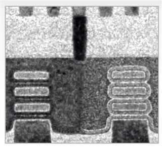
Fig.: Simplified schematics of Silicon-On-Insulator structures. The Buried N(P)-Well (BN(P)W) is a layer dedicated to shielding the electronics from the sensors electric field.

Aknowlegement: This work was financed by the European Union Horizon 2020 Marie Sklodowska-Curie Research and Innovation Staff Exchange program under Grant Agreement no. 645479 (E-JADE) and also by the Polish Ministry of Science and Higher Education from funds for science in the years 2017 – 2018 allocated to an international co-financed project. The authors would like to thank also the operators of the CERN SPS beam line and North Area test facilities.

Opinion Can Israel lead the #opensource code revolution? The Israeli tech scene is based on partnerships, innovation and independent thinking which are all vital in open-source code https://t.co/GdyYArG2sa https://t.co/yG6MPmp7bG


from Twitter https://twitter.com/wladek60

August 31, 2020 at 10:31AM
via IFTTT

Aug 28, 2020

TSMC: All the Processes, All the Fabs

TSMC Technology Symposium: All the Processes, All the Fabs
by Paul McLellan at breakfast-bytes
27 Aug 2020

TSMC has new transistor structure (nanosheet) and new materials such as high mobility channel, 2D, carbon nanotube (CNT). TSMC has already demonstrated at 32Mb nanosheet SRAM fully-functional at 0.46V. It has also identified promising 2D materials such as MoS2 (molybdenum disulfide). At IEDM last year, they disclosed the first BEOL CNT power-gating device integrated with silicon-based CMOS.
Scaling continues with EUV advances with the current generation of scanners. They are also working with ASML (the only supplier of EUV equipment) on High-NA EUV [read more...]


Aug 27, 2020

Chip in the Fields: SBCCI and SBMicro Conferences

Chip in the Fields
C̶a̶m̶p̶i̶n̶a̶s̶,̶ ̶S̶P̶,̶ ̶B̶r̶a̶z̶i̶l̶ ̶ 
Virtual
August 24 to 28, 2020

Due to the COVID-19 pandemic the Chip in the Fields is changed to a virtual event. In 2021 we plan to have again the normal live Chip in the Fields events to be held in Hotel Premium, Campinas, SP, Brazil

The conferences SBCCI and SBMicro started in the early 80’s and since the year 2000 they joined forces, organizing them at the same venue and under a unified fantasy name “Chip in Somewhere”. The somewhere could be the name of the city or a fantasy name related to the region. It started with the name of “Chip in the Jungle”, because it was held in Manaus, the heart of the Amazon forest. 

Along these 21 years of Chip in, gradually other conferences joined the common venue and organization. Nowadays, we are composed of five sister conferences: SBCCI, SBMicro, WCAS, INSCIT and Sforum, as described in the respective call for papers. Due to the COVID-19 pandemic the Chip in the Fields is changed to a virtual event. Detalhes of the program and access link will be made available in the near future. Please follow the conference website for future up-dates.

Keynote Speakers

Kenneth K. O

Texas Analog Center of Excellence and Dept. of ECE,
The University of Texas at Dallas, Richardson, TX

Rajiv V. JoshiT. J. Watson research center, IBM                                         


Sponsored by:

Co-sponsored by:

Organized by:

Supported by:

Silicon Sponsors:

Platinum Sponsors:

Silver Sponsors:


Events:

Aug 26, 2020

[paper] SiC MOSFET Corner and Statistical SPICE Model Generation

SiC MOSFET Corner and Statistical SPICE Model Generation
Canzhong He, James Victory* , Yunpeng Xiao**, Herbert De Vleeschouwer+
Elvis Zheng++, ZhiPing Hu++ 
 ISPSD, September 13-18, 2020, Vienna, Austria
DOI: 10.1109/ISPSD46842.2020.9170091

   Power Design Enablement, ON Semiconductor, Mountain Top, Pennsylvania/USA
 *Power Design Enablement, ON Semiconductor, Aschheim, Germany
**Power Design Enablement, ON Semiconductor, Shanghai, China 
 +Wide Bandgap Technology Development, ON Semiconductor, Oudenaarde, Belgium 
++Product & Test Development Center, ON Semiconductor, Suzhou, China

Abstract: This paper presents a novel approach to generate corner and statistical SPICE models for SiC MOSFETs. The technique is derived from the mature IC industry standard approach known as Backward Propagation of Variance. Physically based, scalable SiC MOSFET SPICE models are required to simulate the correlations between electrical specifications and process variations. The methodologies presented are applicable to other power discrete devices such as super-junction MOSFETs, IGBTs, and GaN HEMTs.

Fig.: SiC MOSFET (a) Cross Section, (b) Subcircuit SPICE Model


Aug 25, 2020

[paper] Native High-k Oxides for 2D Transistors

Yury Yu. Illarionov1,2, Theresia Knobloch1 and Tibor Grasser1
Native high-k oxides for 2D transistors
Nature Electronics vol. 3, pp 442–443 (2020)
Published online: 05 August 2020
DOI: 10.1038/s41928-020-0464-2

1Institute for Microelectronics, TU Wien, Vienna, Austria
2Ioffe Physical-Technical Institute, St Petersburg, Russia

Abstract: The two-dimensional semiconductor Bi2O2Se can be oxidized to create an atomically thin layer of Bi2SeO5 that can be used as the insulator in scaled field-effect transistors.

Fig.: Development of FETs with Bi2O2Se channels and native Bi2SeO5 insulators. a.) Step-by-step oxidation of multilayer Bi2O2Se towards Bi2SeO5 and the crystal structure of the two materials. b.) Cross-sectional scanning transmission electron microscopy image confirming the atomically sharp interface. c.) Schematic of the top-gated devices fabricated with a native gate oxide. d.) Gate transfer characteristics of the devices with a 4.6-nm-thick Bi2SeO5 layer (EOT below 1 nm)

Analog IC Designer's Handbook

by Jean-Francois Debroux
 
Abstract: Analog IC design is one of the particular design activities where designers get feedback on their choices only months after they finish their design and where the cost of even the smallest design change is huge.
This has historically brought the need for new tools such as SPICE, the ancestor of almost all the electric simulators, so as to give feedback on the design choices before actually getting the prototypes. This should also have deeply impacted the design methods, and it has, but the availability of simulators has finally allowed the old “try and fix” method not only to survive but also to stay very popular.
If tools such as electric simulators have gained popularity in most electronic design fields, even out of the IC design world, methods such as the TOP-DOWN approach are not as popular as they should be, especially in the analog design community, even in the analog IC design microcosm. This is probably because this method is felt as difficult to use practically even though most designers agree that it is the right approach.
The goal of this book is to show that the TOP-DOWN approach for analog design is not only valid but that it is one of the most powerful available methods to create good analog design without sacrificing the time to market. This method creates faster and better designs but requires a good understanding of the method itself, of course, but also of the underlying techniques and of the basic design elements.
After a general introduction of the TOP-DOWN method goals and principles in the first part, the second part presents and details analog IC design elements from components to basic building blocks with a strong emphasis on practical aspects. Various additional design techniques are then detailed in the third part. The reader is then ready for the main course, a series of design examples based on the TOP-DOWN method that are grouped in the fourth part. These examples are processed the way they are in real life, from specification to implementation, from general considerations down to implementation details. Analysis of existing circuits is useful for learning but real life design is synthesis, not analysis.
Finally, the fifth part introduces or reminds useful basic concepts and presents the notation in use through the book.
The methods and techniques described in this book have been used by the author through 25 years of analog and mixed signal ICs design experience in various application fields including RF and sensor signal conditioning for various markets such as industrial, automotive and aerospace. The author feels that the method he presents in this book can help many analog electronic designers in their day to day work and hopes it will bring both a deeper understanding of design and a broader view over design activities. [read more...]

Experience: See  Jean-Francois Debroux profile on LinkedIn