Nov 23, 2020

[conference] SISPAD 2020 Technical Program


1st group; (from 9:00 am on Sep. 23 to 11:59 pm on Sep. 28, JST)
Opening and Welcome Remarks Yoshinari Kamakura; (Osaka Inst. Tech., Japan)

Session 1: Plenary Chairperson: Tatsuya Kunikiyo; (Renesas, Japan)
[1-1] Invited Talk "Forefront of Silicon Quantum Computing"; Kohei M. Itoh; (Keio Univ., Japan) pp.1
[1-2] Invited Talk "Ab-initio quantum transport with a basis of unit-cell restricted Bloch functions and the NEGF formalism"; Marco Pala; (CNRS, Univ. Paris-Sud, France) pp.3
[1-3] Invited Talk "Future of Power Electronics from TCAD Perspective"; Terry Ma; (Synopsys, U.S.A.) pp.7

Session 2: Band Structure Chairperson: Chioko Kaneta; (Tohoku Univ., Japan)
[2-1] Invited Talk "Computics Approach toward Clarification of Atomic Reactions during Epitaxial Growth of GaN"; Atsushi Oshiyama; (Nagoya Univ., Japan) pp.11
[2-2] "Estimation of Phonon Mean Free Path in Small-Scaled Si Wire by Monte Carlo Simulation"; Y. Suzuki1, Y. Fujita1, K. Fauziah2, T. Nogita2 H. Ikeda2, T. Watanabe3, Y. Kamakura1; (1 Osaka Inst. Tech., 2 Shizuoka Univ., 3 Waseda Univ., Japan) pp.15
[2-3] "First-principles study of dopant trap level and concentration in Si(110)/a-SiO2 interface"; G.Kang, J. Jeon, J. Kim, H. Ahn, I. Jang, D. Kim; (Samsung Electronics, Korea) pp.19
[2-4] "Energy Band Calculation of Si/Si0.7Ge0.3 Nanopillars in k Space"; M-H Chuang, Y. Li; (National Chiao Tung Univ., Taiwan) pp.23
[2-5] "Full Band Monte Carlo simulation of phonon transfer at interfaces"; N. D. Le1, B. Davier1,2, P. Dollfus1, M. Pala1, A. Bournel1, J. Saint-Martin1; (1 Universite Paris-Saclay, CNRS, France, 2 Univ. Tokyo, Japan) pp.27
[2-6] "First Principle Simulations of Electronic and Optical Properties of a Hydrogen Terminated Diamond Doped by a Molybdenum Oxide Molecule"; J.McGhee, V. P. Georgiev; (Univ. Glasgow, U.K.) pp.31

Session 3: Computational Methodology Chairpersons: Yiming Li; (National Chao Tung Univ., Taiwan)Victor Moroz; (Synopsys, U.S.A.)
[3-1] "High-sigma analysis of DRAM write and retention performance: a TCAD-to-SPICE approach"; S. M. Amoroso1, J. Lee1, A. R. Brown1, P. Asenov1, X. W. Lin2, T. Yang3, V. Moroz2; (1 Synopsys Europe, U.K., 2 Synopsys, U.S.A., 3 Synopsys Taiwan, Taiwan) pp.35
[3-2] "Generative Model Based Adaptive Importance Sampling for Flux Calculations in Process TCAD"; A. Scharinger1, P. Manstetten1, A. Hossinger2, J. Weinbub1; (1 TU Wien, Austria, 2 Silvaco Europe, U.K.) pp.39
[3-3] "Implant heating contribution to amorphous layer: a KMC approach"; P. L. Julliard1,2, P. Dumas1, F. Monsieur1, F. Hilario1, D. Rideau1, A. Hemeryck2, F.Cristiano2; (1 STMicroelectronics, France, 2 LAAS-CNRS, Univ. Toulouse, France) pp.43
[3-4] "Automatic Modeling of Logic Device Performance Based on Machine Learning Utilizing Feature Engineering"; S. Kim, K. Lee, Y. Shin, K. Chang, J. Jeong, S. Baek, M. Kang, K. Cho, D. Kim; (Samsung Electronics, Korea) pp.47
[3-5] "Gummel-cycle Algebraic Multigrid Preconditioning for Large-scale Device Simulations"; H. Koshimoto1, H. Ishimabuchi2, J. Yoo2, Y. Kayama1, S. Yamada1, U. Kwon2, D. S. Kim2; (1 Samsung R&D Inst. Japan, Japan, 2 Samsung Electronics, Korea) pp.51
[3-6] "A continuous cellular automaton method with flux interpolation for two-dimensional electron gas electron transport analysis"; K.Fukuda1, J. Hattori1, H. Asai1, J. Yaita2, J. Kotani2; (1 AIST, Japan, 2 Fujitsu, Japan) pp.55
[3-7] "Geometric Advection Algorithm for Process Emulation"; X.Klemenschits, S. Selberherr, L. Filipovic; (TU Wien, Austria) pp.59

Session 4: Nanowire Chairperson: Susanna Reggiani; (Univ. Bologna, Italy)
[4-1] "Performance and Leakage Analysis of Si and Ge NWFETs Using a Combined Subband BTE and WKB Approach"; Z. Stanojevic, K. Steiner, G. Strof, O. Baumgartner, G. Rzepa, M. Karner; (Global TCAD Solutions, Austria) pp.63
[4-2] "Molecular Dynamics Modeling of the Radial Heat Transfer from Silicon Nanowires"; I. Bejenari1, A. Burenkov1, P. Pichler1, I. Deretzis2, A. La Magna2; (1 Fraunhofer IISB, Germany, 2 CNR-IMM, Italy) pp.67
[4-3] "Advanced simulations on laser annealing: explosive crystallization and phonon transport corrections"; A. Sciuto1,2, I. Deretzis1, S. F. Lombardo1, M. G. Grimaldi2, K. Huet3, B. Curvers3, B. Lespinasse3, A. Verstraete3, I. Bejenari4, A. Burenkov4, P. Pichler4, A. La Magna1; (1 CNR-IMM, Italy, 2 Univ. Catania, Italy, 3 LASSE laser systems and solutions of Europe, France, 4 Fraunhofer IISB, Germany) pp.71
[4-4] "Effect of Unit-Cell Arrangement on performance of Multi-Stage-planar Cavity-free Unileg Thermoelectric Generator Using Silicon Nanowires"; K. Abe1, K. Oda1, M. Tomita1, T. Matsukawa2, T. Matsuki1,2, T. Watanabe1; (1 Waseda Univ., Japan, 2 AIST, Japan) pp.75
[4-5] "Characteristics of Gate-All-Around Silicon Nanowire and Nanosheet MOSFETs with Various Spacers"; S. R. Kola, Y. Li, N. Thoti; (National Chiao Tung Univ., Taiwan) pp.79

Session 5: Material and Geometry Impact Chairpersons: Jun’ichi Hattori; (AIST, Japan)William Vandenberghe; (Univ. Texas at Dallas, U.S.A.)
[5-1] Invited Talk "On the Physical Mechanism of Negative Capacitance Effect in Ferroelectric FET"; Masaharu Kobayashi; (Univ. Tokyo, Japan) pp.83
[5-2] "Undoped SiGe material calibration for numerical laser annealing simulations"; A-S. Royet1, L. Dagault1,2, S. Kerdiles1, P. Acosta-Alba1, J. P. Barnes1, F. Cristiano2, H. Huet3; (1 Univ. Grenoble Alpes, France, 2 LAAS, CNRS Univ. Toulouse, France, 3 Laser Systems & Solutions of Europe, France) pp.89
[5-3] "TCAD simulation for transition metal dichalcogenide channel Tunnel FETs consistent with ab-initio based NEGF calculation"; H. Asai1, T. Kuroda2, K. Fukuda1, J. Hattori1, T. Ikegami1, N. Mori2; (1 AIST, Japan, 2 Osaka Univ., Japan) pp.93
[5-4] "Ab Initio Study of Magnetically Intercalated Tungsten Diselenide"; P. D. Reyntjens1,2,3, S. Tiwari1,2,3, M. L. Van de Put1, B. Sor´ee2,3,4, W. G. Vandenberghe1; (1 Univ. Texas at Dallas, U.S.A., 2 Imec, Belgium, 3 KU Leuven, Belgium, 4 Univ. Antwerp, Belgium) pp.97
[5-5] "A Study of Wiggling AA modeling and Its Impact on Device Performance in Advanced DRAM"; Q.Wang, Y. D. Chen, J. Huang, W. Liu, E. Joseph; (Lam Research, China) pp.101
[5-6] "Reactive Force-Field Molecular Dynamics Study of the Silicon-Germanium Deposition Processes by Plasma Enhanced Chemical Vapor Deposition"; N. Uene1, T. Mabuchi1, M. Zaitsu2, S. Yasuhara2, T. Tokumasu1; (1 Tohoku Univ., Japan, 2 Japan Advanced Chemicals, Japan) pp.105

2nd group; (from 9:00 am on Sep. 28 to 11:59 pm on Oct. 3, JST)
Session 6: Reliability Chairpersons: Markus Karner; (Global TCAD Solutions, Austria)Hajime Tanaka; (Kyoto Univ., Japan)
[6-1] "Universal Feature of Trap-Density Increase in Aged MOSFET and Its Compact Modeling"; F. Avila Herrera1, M. Miura-Mattausch1, T. Iizuka1, H. Kikuchihara1, H. J. Mattausch1, H.Takatsuka2; (1 Hiroshima Univ., Japan, 2 USJC, Japan) pp.109
[6-2] "TCAD Incorporation of Physical Framework to Model N and P BTI in MOSFETs"; R. Tiwari, N. Chowdhury, T. Samadder, S. Mukhopadhyay, N. Parihar, S. Mahapatra; (Indian Inst. Tech., India) pp.113
[6-3] "Benchmarking Charge Trapping Models with NBTI, TDDS and RTN Experiments"; S.Bhagdikar, S. Mahapatra; (Indian Inst. Tech., India) pp.117
[6-4] "A TCAD Framework for Assessing NBTI Impact Under Drain Bias and Self-Heating Effects in Replacement Metal Gate; (RMG)p-FinFETs"; U.Sharma, S. Mahapatra; (Indian Inst. Tech., India) pp.121
[6-5] "Model analysis for effects of spatial and energy profiles of plasma process-induced defects in Si substrate on MOS device performance"; T.Hamano, K. Urabe, K. Eriguchi; (Kyoto Univ., Japan) pp.125

Session 7: Power and Optoelectronic Devices Chairpersons: Blanka Magyari-Kope; (TSMC at U.S.A., U.S.A.)Hideki Minari; (Sony Semiconductor Solutions, Japan)
[7-1] Invited Talk "Modeling and Simulation of Si IGBTs"; Naoyuki Shigyo; (Tokyo Inst. Tech., Japan) pp.129
[7-2] "Full Band Monte Carlo simulations of GaAs p-i-n Avalanche PhotoDiodes: What are the Limits of Nonlocal Impact Ionization Models?"; A. Pilotto1, F. Driussi1, D. Esseni1, L. Selmi2, M. Antonelli3, F. Arfelli3,4, G. Biasiol5, S. Carrato3, G. Cautero6,4, D. De Angelis6, R. H. Menk6,4, C. Nichetti6,3, T. Steinhartova5, P. Palestri1; (1 Univ. Udine, Italy, 2 Univ. Modena and Reggio Emilia, Italy, 3 Univ. Trieste, Italy, 4 INFN, Italy, 5 IOM CNR, Italy, 6 Elettra-Sincrotrone, Italy) pp.131
[7-3] "A technique for phase-detection auto focus under near-infrared-ray incidence in a back-side illuminated CMOS image sensor pixel with selectively grown germanium on silicon"; T. Kunikiyo, H. Sato, T. Kamino, K. Iizuka, K. Sonoda, T. Yamashita; (Renesas Electronics, Japan) pp.137
[7-4] "Investigation of the relationship between current filament movement and local heat generation in IGBTs by using modified avalanche model of TCAD"; T.Suwa; (Toshiba Electronic Devices & Storage, Japan) pp.141
[7-5] "Verilog-A model for avalanche dynamics and quenching in Single-Photon Avalanche Diodes"; Y. Oussaiti1,2, D. Rideau1, J. R. Manouvrier1, V. Quenette1, H. Wehbe-Alause1, B. Mamdy1, A. Lopez1, G. Mugny1, M. Agnew1, E. Lacombe1, J. Grebot1, P. Dollfus2, M. Pala2; (1 STMicroelectronics, France, 2 Centre de Nanosciences et de Nanotechnologies, France) pp.145
[7-6] "A Novel Full-Band Monte Carlo Device Simulator with Real-Space Treatment of the Short-Range Coulomb Interactions for Modeling 4H-SiC Power Devices"; C-Y. Cheng, D. Vasileska; (Arizona State Univ., U.S.A.) pp.149
[7-7] "Tight-binding simulation of optical gain in h-BCN for laser application"; D.Maki, M. Ogawa, S. Souma; (Kobe Univ., Japan) pp.153
[7-8] "Predictive Compact Modeling of Abnormal LDMOS Characteristics Due to Overlap Length Modification"; T. Iizuka1, D. Navarro1, M. Miura-Mattausch1, H. Kikuchihara1, H. J. Mattausch1, D.R. Nestor2; (1 Hiroshima Univ., Japan, 2 Allegro MicroSystems, U.S.A.) pp.157

Session 8: Non-Volatile Memory I Flash and Phase Change Memory Chairperson: Kentaro Kukita; (Kioxia, Japan)
[8-1] "A TCAD Study on Mechanism and Countermeasure for Program Characteristics Degradation of 3D Semicircular Charge Trap Flash Memory"; N. Kariya, M. Tsuda, T. Kurusu, M. Kondo, K. Nishitani, H. Tokuhira, J. Shimokawa, Y. Yokota, H. Tanimoto, S. Onoue, Y. Shimada, T. Kato, K. Hosotani, F. Arai, M. Fujiwara, Y.Uchiyama, K. Ohuchi; (Kioxia, Japan) pp.161
[8-2] "Impact of Random Phase Distribution in 3D Vertical NAND Architecture of Ferroelectric Transistors on In-Memory Computing"; G.Choe, W. Shim, J. Hur, A. I. Khan, S. Yu; (Georgia Inst. Tech., U.S.A.) pp.165
[8-3] "TCAD Modeling and Optimization of 28nm HKMG ESF3 Flash Memory"; A. Zaka, T. Herrmann, R. Richter, S. Duenkel, R. Jain; (GLOBALFOUNDRIES, Germany) pp.69
[8-4] "Coupling the Multi Phase-Field Method with an Electro-Thermal Solver to Simulate Phase Change Mechanisms in Ge-rich GST based PCM"; R. Bayle1,2,3, O. Cueto1, S. Blonkowski1, T. Philippe3, H. Henry3, M. Plappa3; (1 CEA-LETI, France, 2 STMicroelectronics, France, 3 Ecole Polytechnique, France) pp.173

Session 9: Transport Chairperson: Christoph Jungemann; (Univ. Aachen, Germany)
[9-1] "Efficient partitioning of surface Green’s function: toward ab initio contact resistance study"; G. Gandus1,2, Y. Lee2, D. Passerone1, M. Luisier2; (1 nanotech@surfaces; (EMPA), Switzerland, 2 Integrated Systems Laboratory; (ETH Zurich), Switzerland) pp.177
[9-2] "Quantum transport in Si: P δ-layer wires"; J. P. Mendez, D. Mamaluy, X. Gao, L. Tracy, E. Anderson, D. Campbell, J. Ivie, T.-M. Lu, S.Schmucker, S. Misra; (Sandia National Laboratories, U.S.A.) pp.181
[9-3] "Analytical Formulae for the Surface Green’s Functions of Graphene and 1T’ MoS2 Nanoribbons"; H.Kosina, V. Sverdlov; (TU Wien, Austria) pp.185
[9-4] "Numerical Solution of the Constrained Wigner Equation"; R.Kosik, J. Cervenka, H. Kosina; (TU Wien, Austria) pp.189
[9-5] "Calibrated Si Mobility and Incomplete Ionization Models with Field Dependent Ionization Energy for Cryogenic Simulations"; H. Y. Wong; (San Jose State Univ., U.S.A.) pp.193

Session 10: Non-Volatile Memory II ReRAM and MRAM Chairperson: Uihui Kwon; (Samsung, Korea)
[10-1] "Monte Carlo Simulation of a Three-Terminal RRAM with Applications to Neuromorphic Computing"; A.Balasingam, A. Levy, H. Li, P. Raina; (Stanford Univ., U.S.A.) pp.197
[10-2] "Fully Analog ReRAM Neuromorphic Circuit Optimization using DTCO Simulation Framework"; A. Nguyen1, H. Nguyen1, S. Venimadhavan1, A. Venkattraman2, D. Parent1, H. Y. Wong1; (1 San Jose State Univ., U.S.A., 2 Univ. California Merced, U.S.A.) pp.201
[10-3] "Effect of Shape Deformation due to Edge Roughness in Spin-Orbit Torque Magnetoresistive Random-Access Memory"; Byun, D. H. Kang, M. Shin; (KAIST, Korea) #205
[10-4] "Computation of Torques in Magnetic Tunnel Junctions through Spin and Charge Transport Modeling"; S. Fiorentini1, J. Ender1, M. Mohamedou1, R. Orio1, S. Selberherr1, W. Goes2, V. Sverdlov1; (1 TU Wien, Austria, 2 Silvaco Europe, U.K.) pp.209
[10-5] "Efficient Demagnetizing Field Calculation for Disconnected Complex Geometries in STT-MRAM Cells"; J. Ender1, M. Mohamedou1, S. Fiorentini1, R. Orio1, S. Selberherr1, W. Goes2, V. Sverdlov1; (1 TU Wien, Austria, 2 Silvaco Europe, U.K.) pp.213
[10-6] "Properties of Conductive Oxygen Vacancies and Compact Modeling of IV Characteristics in HfO2 Resistive Random-Access-Memories"; J.Park, M.-J. Kim, J.-H. Jang, S.-M. Hong; (Gwangju Inst. Sci. Tech., Korea) pp.217

Session 11: High Speed Switching Devices Chairpersons: Akira Hiroki; (Kyoto Inst. Tech., Japan)Sebastien Martinie; (CEA-LETI, France)
[11-1] "MOS-like approach for compact modeling of HEMT transistor"; A. Vaysset, S. Martinie, F. Triozon, O. Rozeau, M.-A. Jaud, R. Escoffier, T. Poiroux; (CEA, LETI, Univ. Grenoble Alpes, France) pp.221
[11-2] "Compact modeling of gate leakage phenomenon in GaN HEMTs"; K. Li1,3, E. Yagyu2, H. Saito2, K. H. Teo1; (1 Mitsubishi Electric Research Labs, U.S.A., 2 Mitsubishi Electric Corp., Japan, 3 Univ. Illinois at Urbana-Champaign, U.S.A.) pp.225
[11-3] "Effect of Atomic Interface on Tunnel Barrier in Ferroelectric HfO2 Tunnel Junctions"; J.Seo, M. Shin; (KAIST, Korea) pp.229
[11-4] "Surge Current Capability in lateral AlGaN/GaN Hybrid Anode Diodes with p-GaN/Schottky Anode"; G. Atmaca1, M.-A. Jaud1, J. Buckley1, R. Gwoziecki1, A. Yvon2, E. Collard2, M. Plissonnier1, T.Poiroux1; (1 CEA, LETI, Univ. Grenoble Alpes, France, 2 STMicroelectronics, France) pp.233
[11-5] "Dynamic Simulation of Write ‘1’ Operation in the Bi-stable 1-Transistor SRAM Cell"; T. Dutta1, F. Adamu-Lema1, A. Asenov1, Y. Widjaja2, V. Nebesnyi3; (1 Semiwise, U.K., 2 Zeno Semiconductor, 3 MCPG) pp.237
[11-6] "Simulation of gated GaAs-AlGaAs resonant tunneling diodes for tunable terahertz communication applications"; V. Georgiev, A. Sengupta, P. Maciazek, O. Badami, C. Medina-Bailon, T. Dutta, F.Adamu-Lema, A. Asenov; (Univ. Glasgow, U. K.) pp.241
[11-7] "Theoretical Study of Double-Heterojunction AlGaN/GaN/InGaN/δ-doped HEMTs for Improved Transconductance Linearity"; T.-H. Yu; (Inforsight Computing, Taiwan) pp.245
[11-8] "Nanoscale FET: How To Make Atomistic Simulation Versatile, Predictive, and Fast at 5nm Node and Below"; P. Blaise1, U. Kapoor1, M. Townsend1, E. Guichard1, J. Charles2, D. A. Lemus2, T. Kubis2; (1 Silvaco, U.S.A., 2 Purdue Univ., U.S.A.) pp.249

3rd group; (from 9:00 am on Oct. 1 to 11:59 pm on Oct. 6, JST)
Session 12: Emerging Devices Chairpersons: Andres Godoy; (Univ. Granada, Spain)Sung-Ming Hong; (Gwangju Inst. Sci. Tech., Korea)
[12-1] Invited Talk "TCAD-Assisted MultiPhysics Modeling & Simulation for Accelerating Silicon Quantum Dot Qubit Design"; Fahd Ayyalil Mohiyaddin; (imec, Belgium) pp.253
[12-2] "Physics-augmented Neural Compact Model for Emerging Device Technologies"; Y.Kim, S. Myung, J. Ryu, C. Jeong, D. S. Kim; (Samsung Electronics, Korea) pp.257
[12-3] "A Modeling Study on Performance of a CNOT Gate Devices based on Electrode-driven Si DQD Structures"; H.Ryu, J.-H. Kang; (Korea Inst. Sci. Tech. Info., Korea) pp.261
[12-4] "Simulation and Evaluation of Plasmonic Circuits"; M.Fukuda, Y. Ishikawa; (Toyohashi, Univ. Tech., Japan) pp.265
[12-5] "Numerical study of surface chemical reactions in 2D-FET based pH sensors"; A. Toral-Lopez1, E. G. Marin1, J. Cuesta1, F. G. Ruiz1, F. Pasadas2, A. Mediana-Rull1, A.Godoy1; (1 Univ. Granada, Spain, 2 Univ. Autonoma Barcelona, Spain) pp.269
[12-6] "A Combined First Principle and Kinetic Monte Carlo Study of Polyoxometalates Based Molecular Memory Devices"; P. Lapham, O. Badami, C. Medina-Bailon, F. Adamu-Lema, T. Dutta, V. Georgiev, A.Asenov; (Univ. Glasgow, U.K.) pp.273
[12-7] "Modeling Assisted Room Temperature Operation of Atomic Precision Advanced Manufacturing; (APAM)Devices"; X. Gao, L. Tracy, E. Anderson, DeAnna Campbell, J. Ivie, T.-M. Lu, D. Mamaluy, S.Schmucker, S. Misra; (Sandia National Lab., U.S.A.) pp.277

Session 13: 2D and Nano System I Chairperson: Jeff Wu; (TSMC, Taiwan)
[13-1] "Effects of the Dielectric Environment on Electronic Transport in Monolayer MoS2: Screening and Remote Phonon Scattering"; M. L. Van de Put, G. Gaddemane, S. Gopalan, M. V. Fischetti; (Univ. Texas at Dallas, U.S.A.) pp.281
[13-2] "Impact of Schottky Barrier on the Performance of Two-Dimensional Material Transistors"; S.-K. Su, J. Cai, E. Chen, L.-J. Li, H.-S. Philip Wong; (TSMC, Taiwan) pp.285
[13-3] "AC NEGF Simulation of Nanosheet MOSFETs"; S.-M. Hong, P.-H. Ahn; (Gwangju Inst. Sci. Tech., Korea) pp.289
[13-4] "Enhanced Capabilities of the Nano-Electronic Simulation Software; (NESS)"; C. Medina-Bailon, O. Badami, H. Carrillo-Nunez, T. Dutta, D. Nagy, F. Adamu-Lema, V.Georgiev, A. Asenov; (Univ. Glasgow, U.K.) pp.293
[13-5] "Electrostatic Potential Profile Generator for Two-Dimensional Semiconductor Devices"; S.-C. Han, J. Choi, S.-M. Hong; (Gwangju Inst. Sci. Tech., Korea) pp.297

Session 14: FET Devices and Design Technology Co-Optimization Chairpersons: Mehdi Bazizi,; (Applied Materials, U.S.A.)Lado Filipovic; (TU Wien, Austria)
[14-1] Invited Talk "Agile Pathfinding Technology Prototyping: the Hunt for Directional Correctness"; Daniel Chanemougame; (TEL at Albany, U.S.A.) pp.301
[14-2] "Self-Aligned Single Diffusion Break Technology Optimization Through Material Engineering for Advanced CMOS Nodes"; A. Pal, E. M. Bazizi, L. Jiang, M. Saremi, B. Alexander, B. Ayyagari-Sangamalli; (Applied Materials, U.S.A.) pp.307
[14-3] "L-UTSOI: A compact model for low-power analog and digital applications in FDSOI technology"; S. Martinie1, O. Rozeau1, T. Poiroux1, P. Scheer1, S. E. Ghouli2, M. Kang3, A. Juge2, H. Lee3; (1 CEA, LETI, Univ. Grenoble Alpes, France, 2 STMicroelectronics, France, 3 Samsung, Korea) pp.311
[14-4] "Electromigration Model for Platinum Hotplates"; L.Filipovic; (TU Wien, Austria). pp.315
[14-5] "Compact Modeling of Radiation Effects in Thin-Layer SOI-MOSFETs"; M. Miura-Mattausch, H. Kikuchihara, D. Navarro, T. Iizuka, H. J. Mattausch; (Hiroshima Univ., Japan). pp.319
[14-6] "Complementary FET Device and Circuit Level Evaluation Using Fin-Based and Sheet-Based Configurations Targeting 3nm Node and Beyond"; L. Jiang, A. Pal, E. M. Bazizi, M. Saremi, R. He, B. Alexander, B. Ayyagari-Sangamalli; (Applied Materials, U.S.A.) pp.323
[14-7] "Via Size Optimization for Optimum Circuit Performance at 3 nm node"; S. Mittal1, A. Pal2, M. Saremi2, E. M. Bazizi2, B. Alexander2, B. Ayyagari-Sangamalli2; (1 Applied Materials, India, 2 Applied Materials, U.S.A.) pp.327
[14-8] "Time-Resolved Mode Space based Quantum-Liouville type Equations applied onto DGFETs"; L.Schulz, D. Schulz; (TU Dortmund, Germany) pp.331

Session 15: Machine Learning Chairpersons: Satofumi Souma; (Kobe Univ., Japan)Hiuyung Wong; (San Jose State Univ., U.S.A.)
[15-1] Invited Talk "Power Device Degradation Estimation by Machine Learning of Gate Waveforms"; Makoto Takamiya; (Univ. Tokyo, Japan) pp.335
[15-2] "Machine Learning Prediction of Formation Energies in a-SiO2"; D.Milardovich, M. Jech, D. Waldhoer, M. Waltl, T. Grasser; (TU Wien, Austria) pp.339
[15-3] "Novel Optimization Method using Machine-learning for Device and Process Competitiveness of BCD Process"; J. Kim, J.-H. Yoo, J. Jung, K. Kim, J. Bae, Y.-S. Kim, O.-K. Kwon, U.-H. Kwon, D.-S. Kim; (Samsung Electronics, Korea) pp.343
[15-4] "Real-Time TCAD: a new paradigm for TCAD in the artificial intelligence era"; S. Myung, J. Kim, Y. Jeon, W. Jang, J. Kim, S Han, K.-H. Baek, J. Ryu, Y.-S. Kim, J. Doh, C.Jeong, D. -S. Kim; (Samsung Electronics, Korea) pp.347
[15-5] "Application of Noise to Avoid Overfitting in TCAD Augmented Machine Learning"; S. S. Raju1, B. Wang2, K. Mehta1, M. Xiao2, Y. Zhang2, H.-Y. Wong1; (1 San Jose Univ., U.S.A., 2 Virginia Polytech. Inst. State Univ., U.S.A.) pp.351
[15-6] "Automatic Device Model Parameter Extractions via Hybrid Intelligent Methodology"; C.-C. Liu, Y. Li, Y.-S. Yang, C.-Y. Chen, M.-H. Chuang; (National Chiao Tung Univ., Taiwan) pp.355
[15-7] "Physics-Informed Graph Neural Network for Circuit Compact Model Development"; X. Gao, A. Huang, N. Trask, S. Reza; (Sandia National Lab., U.S.A.) pp.359

Session 16: 2D and Nano System II Chairperson: Frank Register; (Univ. Texas at Austin, U.S.A.)
[16-1] "Theoretical study of electronic transport in monolayer SnSe"; S. Gopalan1, G. Gaddemane2, M. L. Van de Put1, M. V. Fischetti1; (1 Univ. Texas at Dallas, U.S.A., 2 imec, Belgium) pp.363
[16-2] "Transient simulation of graphene FET gated by electrolyte medium"; K. Arihori1, M. Ogawa1, S. Souma1, J. Sato-Iwanaga2, M. Suzuki2; (1 Kobe Univ., Japan, 2 Panasonic, Japan) pp.367
[16-3] "Quantum Transport Simulations of Phosphorene Nanoribbon MOSFETs: Effects of Metal Contacts, Ballisticity and Series Resistance"; M.Poljak, Mislav Matic; (Univ. Zagreb, Croatia) pp.371
[16-4] "High-Performance Metal-Ferroelectric-Semiconductor Nanosheet Line Tunneling Field Effect Transistors with Strained SiGe"; N. Thoti1, Y. Li1, S. R. Kola1, S. Samukawa2; (1 National Chaio Tung Univ., Taiwan, 2 Tohoku Univ., Japan) pp.375
[16-5] "A First-Principles Study on the Strain-induced Localized Electronic Properties of Dumbbell-shape Graphene Nanoribbon for Highly Sensitive Strain Sensors"; Q.Zhang, K. Suzuki, H. Miura; (Tohoku Univ., Japan) pp.379

Late News Chairperson: Tatsuya Kunikiyo; (Renesas Electronics, Japan)
LN "Multiband Phase Space Operator for Narrow Bandgap Semiconductor Devices"; L.Schulz, D. Schulz; (TU Dortmund, Germany) pp.383

[conference] CADTFT2020 Final Program

Final Program
11th International Conference on Computer Aided Design for Thin-Film Transistor Technologies
November 9-11, 2020 
http://www.cadtft2020.org/

2020/11/09 Monday Day 1 (1/3)
Tutorial Session 1 (Chair: Kai Wang)
[T1] Karim S. Karim Uni. Waterloo; Canada;"Next Generation Diagnostic X-ray Imagers for Scalable and Sustainable Healthcare"
[T2] Samar Saha IEEE Electron Device Society "What can we learn from Fin-FET?"

Poster Session (Chair: Di Geng)
[P1] Guan Ying Wang Uni. Toronto; Canada;"Electrolyte-gated Field Effect Transistors in Biological Sensing"
[P2] Mihir Srivastava Avantika University; India;"A Simple Approach to Estimate Performance Deteriorations of Circuits with Non-Ohmic TFTs"
[P3] Zhaohan Peng National Center for Nanoscience and Technology CAS; China;"High Electrical and Mechanical Stability of IGZO Transistor Arrays on Flexible Substrate"
[P4] Penglong Chen Chongqing Uni. Posts and Telecommunications; China;"A New Voltage-Programming IGZO TFT AMOLED Pixel Compensation Circuit"
[P5] Fengjing Liu National Center for Nanoscience and Technology CAS; China;"Organic-inorganic Hybrid Complementary Inverter Based Photodetector with Amplified Voltage-output"
[P6] Eva Bestelink Uni. Surrey; UK;"Source-Gated Transistor Current Mirrors with Negative Temperature Dependence"

Tutorial Session 2 (Chair: Xiaojun Guo)
[T3] Sanjiv Sambandan Indian Institute of Science; India;"Challenges and Solutions to Analog Integrated Circuit Design with Thin Film Transistors"
[T4] Arokia Nathan Uni. Cambridge; UK;"TFT Circuits for Signal Processing"
[T5] Yvan Bonnassieux Ecole Polytechnique; France;"Compact Modeling of Organic Field-Effect Transistors"
[T6] Slobodan Mijalkovic Silvaco Europe; UK;"Compact Modeling of Hysteretic Phenomena"

2020/11/10 Tuesday Day 2 (2/3) 
Opening Plenary Session 1 (Ling Li)
[P1] Feng Qin Tianma Microelectronics; China;"TFT Foundry Multi-Project"
[P2] Yanfeng Li Primarius Technologies; China;"Enabling DTCO with a Complete EDA Ecosystem from Data to Simulation"

Session 1 Device Modeling and Characterization (Chair: Liling Zhang)
[1-1] Ta-Ya Chu National Research Council; Canada;"Pinch-Off Mobility Extraction for Organic Thin-Film Transistors"
[1-2] Sungyeop Jung Seoul National University; South Korea;"Organic Thin-Film Transistor Compact Modeling"
[1-3] Wanling Deng Jinan University; China;"Modelling Method based on BP Neural Network and Artificial Bee Colony Algorithm for Metal-oxide Thin-Film Transistors"
[1-4] Jumbum Park Ecole Polytechnique; France;"Validation of Power-law Drain Current Model for Coplanar OFETs at Various Temperatures"
[1-5] Mingxiang Wang Soochow University; China;"Comparative Study of Dynamic Degradation of Oxide TFTs in ESL or EMMO Structure"

Session 2 Device Design and Technology (Chair: Chuan Liu)
[2-1] Paddy Chan The Uni. Hong Kong; China;"Solution Processed Organic Monolayer Field Effect Transistors"
[2-2] Sanjiv Sambandan Indian Institute of Science; India;"Adaptive Dielectric Thin Film Transistors - A New Interface Device for Large Area, Flexible and Wearable Electronics"
[2-3] Aiming Song Uni. Manchester; UK;"Thin Film Transistors Based on Semiconductors and Semimetals"
[2-4] Andrew Flewitt Uni. Cambridge; UK;"Quantitative Analysis of the Bias Stress-Induced Threshold Voltage Shift in TFTs incorporating Disordered Materials"

Session 3 Device and Circuit Interaction (Chair: Chair: Xueqing Li)
[3-1] Niko Muenzenrieder Free University Bolzano; Italy;"Tools and Strategies to Optimize the Electrical and Mechanical Properties of Flexible TFTs"
[3-2] Ya-Hsiang Tai NCTU "Acquiring Differential Light Signal with TFT Sensing Array"
[3-4] Radu Sporea Uni. Surrey; UK;"Multimodal Thin-film Transistors: an Opportunity for Analog Signal Processing and Computation"
[3-5] Chen Jiang Uni. Cambridge; UK;"All-Inkjet-Printed Ultra-low-Power Organic Thin-Film Transistors for Electrophysiological Monitoring"
[3-6] Gerwin Gelinck Holst Centre, TNO; Netherland;"Organic Photodiodes for Imaging and Sensing Applications"

Plenary Session 2 ( Chair: Arokia Nathan)
[P3] Zhigang Shuai Tsinghua University; China;"First-principles Methods for Investigating Carrier Transport and Light-Emitting in Organic Semiconductors"
[P4] Ahmed Nejim Silvaco Europe; UK;"Modelling Thin Film Electronics - Recent TCAD Developments"

2020/11/11 Wednesday Day 3 (3/3)
Plenary Session 3 (Chair: Ling Li)
[P5] Jin Jang Kyung Hee University; South Korea;"Mechanical Stabilities of TFTs on Flexible Substrate"
[P6] Tim Cheng Hong Kong Uni. Science and Technology; China;"Ultra-thin and Robust Skin Electronics for High Quality and Continuous Skin-Sensor-Silicon Interfacing"

Session 4 Material Design & Processing ( Chair: Hang Zhou)
[4-1] Simon Rongdeau-Gagne Uni. Windsor; Canada;"Design of Stretchable and Self-healable Polymers for Fabrication of Stretchable Transistors"
[4-2] Myung-Gil Kim Sungkyunkwan University; South Korea;"Solution-Processing of Hybrid Materials for Flexible Electronics and Sensors"
[4-3] Min Zhang Peking University; China;"High-Performance Intrinsically Soft Thin Film Transistors"
[4-4] Xiaochen Ren Tianjin University; China;"Solution Processed Organic Crystalline Arrays for High-performance Organic Field-effect Transistors"

Session 5 Circuit Design (Chair: Hanbin Ma)
[5-1] Yuanfeng Chen Kyung Hee University; South Korea;"Gate Driver using Low-Temperature Poly-Si Oxide TFTs with Mobility Compensation"
[5-2] Congwei Liao Peking University; China;"Thin-film Transistor Integrated Gate Driver Circuit Design for in-Cell Touch Display"
[5-3] Seung-Woo Lee Kyung Hee University; South Korea;"Fault-tolerant Integrated Scan Driver Circuit for Implantable Bio-sensor Systems"
[5-6] Hongge Li Beihang University; China;"A High-precision Low Power Driver Circuit for Printed Display"

Session 6 Emerging Applications (Chair: Kai Wang)
[6-1] Xueqing Li Tsinghua University; China;"Organized by: Co-organized by: Technical Sponsor: "Emerging Ferroelectric Memory and Computing"
[6-2] Hanbin Ma SIBET CAS; China;"Active Matrix Digital Microfluidics Lab-on-a-Chip with Drain-offset a-Si TFTs"
[6-3] Xiao Gong National Uni. Singapore; Singapore;"Amorphous Metal Oxide-based TFTs for 3D Monolithic Integration Nano-electronic Systems"
[6-4] Zhe Liu Hangzhou LinkZill Technology Co. Ltd; China;"TFT-based System for Beyond-display Applications"
[6-5] Hang Zhou Peking University Shenzhen Graduate School; China;"Perovskite-IGZO Hybrid Phototransistor for Photodetection and Image Sensor"

Plenary Session 4 (Chair: Arokia Nathan)
[P7] Benjamin Iñiguez Universitat Rovirai Virgili; Spain;"Modeling of Low Frequency Noise in Organic and Oxide TFTs"

China-Europe Dialogue on TFT Compact Modeling 
  • Benjamin Iñiguez Universitat Rovirai Virgili; Spain; "European DOMINO Project on TFT Compact Modeling"
  • Shijia Lin Huada Empyrean Software; China; "Advances in TFT Device and Reliability Modeling"
Closing Remarks

Nov 21, 2020

[mos-ak] [Final Program] 13th International MOS-AK Workshop; Silicon Valley, Dec.10-11 2020

Together with THM Giessen, the MOS-AK workshop online host and IEEE Young Professionals (Germany), technical program promoter as well as all the Extended MOS-AK TPC Committee, we have the pleasure to invite to consecutive, 13th International MOS-AK Workshop is Silicon Valley which will be Virtual/Online event using Zoom platform.

Scheduled, subsequent 13th MOS-AK SPICE/Compact Modeling Workshop organized in the Silicon Valley, aims to strengthen a network and discussion forum among experts in the field, enhance open platform for information exchange related to compact/SPICE modeling and Verilog-A standardization, bring people in the compact modeling field together, as well as obtain feedback from technology developers, circuit designers, and TCAD/EDA tool developers and vendors. 

The MOS-AK workshop program is available online

Venue: Virtual/Online Workshop on Zoom platform
  • virtual session 11:00 - 14:00 (PST) on Dec.10, 2020
  • virtual session 11:00 - 14:00 (PST) on Dec.11, 2020
Online free Registration is open, now. Registered participant will receive Zoom meeting invitation.
(any related enquiries can be sent to registration@mos-ak.org)

Postworkshop Publications:
Selected best MOS-AK technical presentation will be recommended for further publication in a special Solid State Electronics issue on compact modeling 

W.Grabinski on the behalf of International MOS-AK Committee
WG20112020

--
You received this message because you are subscribed to the Google Groups "mos-ak" group.
To unsubscribe from this group and stop receiving emails from it, send an email to mos-ak+unsubscribe@googlegroups.com.
To view this discussion on the web visit https://groups.google.com/d/msgid/mos-ak/3f3582a0-987b-4700-9dc0-fe3e90f1ce49n%40googlegroups.com.

Nov 20, 2020

#EspoTek Labrador: a complete arsenal of electronic engineering instruments: an oscilloscope, function generator, power supply, logic analyzer and multimeter. https://t.co/KjhalAi080 #semi https://t.co/CC6pt5DxiD


from Twitter https://twitter.com/wladek60

November 20, 2020 at 02:29PM
via IFTTT

[Launch Event] EMPHASIS University of Cyprus

LAUNCH EVENT: November 25, 2020 10:00-13:30EET

EMPHASIS is a multidisciplinary research centre involving departments from the School of Engineering and School of Pure & Applied Sciences from the University of Cyprus. Join us online to learn more about our labs' research in the key enabling technologies behind the digital revolution: electronics, microwaves & antennas, photonics and sensors.

SCHEDULE: (Eastern European Time)
10:00–10:10: Introduction 
Prof.Tasos Christofides, Rector of the University of Cyprus
10:10–10:20: Introductory Remarks
Dr.Nikolas Mastroyiannopoulos, Chief Scientist for Research and Innovation
10:20–10:50: EMPHASIS Research Centre: Vision & Goals,
Prof.Stavros Iezekiel, Acting Director of EMPHASIS
BREAK
11:00–11:30: EMPHASIS Research Laboratory Presentations
11:30–13.30: Presentation of Selected Research Projects in Electronics, Microwaves & Antennas, Photonics and Sensors
SESSION1: 11:30-12:30
• Medical Electronics,
Prof.Julius Georgiou
• Sensors for Precision Agriculture, 
Dr.Marios Sophocleous
• Resveratrolloaded Polymeric Miceles for Theranostic Targeting of Breast Cancer Cels, 
Dr.Yiota Grigoriou
• White Light Emitting Structures Based on II-Nitrides and Lead Halide Perovskite Nanocrystals,
Dr.Modestos Athanasiou
• Multi-bacteria,Multi-antibiotic Testing Using Surface Enhanced Raman Spectroscopy
(SERS)forUrinary Tract Infection (UTI)Diagnosis, 
Dr.Katerina Hadjigeorgiou
BREAK
SESSION2: 12:30-13:30
• Electric-Field Measurements of Microwave Circuits,
Dr.Haris Votsi
• Integrated Circuits for RF Metasurfaces, 
Loukas Petrou/Kypros Kossifos
• Influence of Carriers in Spin Pumping in Organic Semiconductors, 
Constantinos Nicolaides
• Microwave Photonics for Space,
Georgios Charalambous
• Wireless Power Transfer (WPT) and Far-Field RF Energy Harvesting,
Dr.Abdul Quddious

FOR MORE INFORMATION: www.emphasis.ucy.ac.cy/launch-event


[paper] Characterization of ultrathin FDSOI devices using subthreshold slope method

Teimuraz Mchedlidze1, and Elke Erben2
Characterization of ultrathin FDSOI devices using subthreshold slope method
Phys. Status Solidi A. Accepted Manuscript
DOI: 10.1002/pssa.202000625

1 TU Dresden, Germany
2 Globalfoundries, Dresden, Germany

Abstract: The subthreshold current-voltage (subthreshold slope) characteristic of fully depleted silicon-on-insulator high-k dielectric-metal gate field-effect transistor is applied for evaluation of the interface traps located at both, the front and back channels. The proposed characterization method allows an estimation of averaged trap densities separately for the front and the back interfaces of the channel. Performing subthreshold slope measurements at several temperatures allow the extraction of the energy distributions of the interface trap densities for both interfaces and obtaining essential characteristics of the stack.

Fig: Results of ID(VGF,k,T) measurements for EG sample. At each temperature 
(200, 300 and 400K) a group of curves contains data for eight k values
(k = 0 to 3 with step 0.5 and kOC; solid curve). 

Acknowledgements: The authors would like to acknowledge funding of the study in the frames of the IPCEI WIN- FDSOI project from Global Foundries. We want to thank Jörg Weber (TU Dresden), Luca Pirro (Global Foundries) and Rolf Öttking (AQ Computare, Chemnitz) for thoughtful discussions and suggestions.


Nov 19, 2020

#Nanoscale #Schottky #diodes fabricated via adhesion lithography https://t.co/dkeSdlinNP #semi https://t.co/u353DjjCVP


from Twitter https://twitter.com/wladek60

November 19, 2020 at 04:38PM
via IFTTT

#India Has $100 Billion Opportunity Through Domestic #Manufacturing Of Tablets, Laptops [ICEA] https://t.co/YIekOOiFME #semi https://t.co/S0rb3I1jXA


from Twitter https://twitter.com/wladek60

November 19, 2020 at 04:37PM
via IFTTT

[paper] Compact Model for Power MOSFET

Abdelghafour Galadi
PSPICE compact model for power MOSFET based on manufacturer datasheet
DOI:10.1088/1757-899X/948/1/012007

National School of Applied Sciences of Safi, Cadi Ayyad University, Marrakech (MA)

Abstract: In this paper, large signal model for power MOSFET devices is presented. The proposed model includes quasi-saturation effect and describes accurately the electrical behavior of the power MOSFET devices. The large signal model elements will be provided based on the device structure. Furthermore, the model parameters are extracted from measurements considering the voltages depending effect of the nonlinear gate-source, gate-drain and drain-source interelectrode capacitances. Excellent agreements will be shown between the simulated and the datasheet data. Finally, a description of the model will be provided along with the parameter extraction procedure.
Fig: a) Conventional power MOSFET structure with b) its subcircuit elements. 


[paper] HEMT RF/Analog Performance

M. Khaouani1,H. Bencherif2, A. Hamdoune1, A. Belarbi3, Z. Kourdi4
RF/analog Performance Assessment of High Frequency, Low Power In0.3Al0.7As/InAs/InSb/In0.3Al0.7As HEMT Under High Temperature Effect
Transactions on Electrical and Electronic Materials
The Korean Institute of Electrical and Electronic Material Engineers 2020
DOI: 10.1007/s42341-020-00250-8

1 Department of Genie Electric and Electronics, Unit Research of Material and Renewable Energies, University Aboubek Belkaid, Tlemcen, Algeria
2 LAAAS Laboratory, University of Batna 2, Batna, Algeria
3 Center Exploitation Telecommunication Satellite– Bouchaoui-Alger, Algeria Space Agency, Algiers, Algeria
4 Center Exploitation Telecommunication Satellite– Oran-Alger, Algeria Space Agency, Algiers, Algeria


In0.3Al0.7As/InAs/InSb/In0.3Al0.7As In this paper, we performed a Pseudo-morphic High Electron Mobility Transistors (pHEMT) In0.3Al0.7As/InAs/InSb/In0.3Al0.7As using commercial TCAD. RF and analog electrical characteristics are assessed under high temperature effect. The impact of the temperature is evaluated referring to a device at room temperature. In particular, the threshold voltage (Vth), transconductance (gm), and Ion/Ioff ratio are calculated in the temperature range of 300K to 700K. The primary device exhibits a drain current of 950mA, a Vth of -1.75V, a high value of gm of 650 mS/mm, Ion/Ioff ratio of 1E6, a transition frequency (fT) of 790GHz, and a maximum frequency (fmax) of 1.4THz. The achieved results show that increasing temperature act to decrease current, reduce gm, and Ion/Ioff ratio. In more detail high temperature causes a phonon scattering mechanism happening that determine in turn a reduced drain current and shift positively the threshold voltage resulting in hindering the device DC/AC capability. 
Fig: 2D cross section of In0.3Al0.7As/InAs/InSb/In0.3Al0.7AsAs PHEMT


Nov 18, 2020

[paper] Verilog-A Ion Sensitive FET for pH Sensor

Megha Agrawal, Nidhi Agrawal, Alpana Agarwal and Anil K. Saini*
Modeling of Ion Sensitive Field Effect Transistor for pH Sensor using Verilog-A
 Recent Advancement in Communication System & Image Processing
RACISP-2012 at: BKBIET, Pilani

Thapar University, PATIALA – 147004, Punjab
*Central Electronics Engineering Research Institute, PILANI – 333031, Rajasthan

Abstract: ISFET semiconductor technology enables the design of true solid state pH sensor. An ISFET can be modeled by considering it as two fully uncoupled stages: an electronic stage i.e., the MOSFET which is the starting structure of the ISFET and an Electro-chemical stage i.e., the electrolyte–insulator interface which is pH dependent. This paper describes the modeling of ISFET for pH measurement using Verilog A which is compatible with cadence environment. Any change in pH directly affects the threshold voltage of ISFET. To measure this change in pH, ISFET is configured in such a way so that change in threshold voltage can be directly detected. For this purpose a sensing read-out has been designed using Gate complementary ISFET/MOSFET pair (CIMP) technique. Simulated result shows good linearity between output voltage of sensing readout circuit with pH variation for the range of 1 to12. The ISFET is thermally instable due to semiconductor properties and pH dependency on temperature, which in turn affects the pH reading of the solution at a temperature other than room temperature with slope of +0.69mV/0C, +1.25mV/0C and +1.60mV/0C respectively for pH= 4, for pH=7 and for pH=10.
Fig: a) n-channel ISFET structure and b) its equivalent electric circuit [ref]

Acknowledgment: The work is financially supported by Department of Information Technology, Ministry of Communication & Information Technology, Government of India, under SMDP-VLSI (Phase II) project.

[ref] Sergio Martinoia, Giuseppe Massobrio, “A Behavioral Macromodel of the ISFET in SPICE,” Sensors and Actuators B, Vol. 62, pp. 182–189, 2000

Appendix A

// Verilog-A Code for ISFET [ref]
`include "constants.vams"
`include "disciplines.vams"
module ISFET(ref,gm,ph);
inout ref,gm,ph;
electrical ref,gm,ph;
real EPH;
real T;
electrical node;
electrical x,y;
// PARAMETERS FOR ISFET
parameter real NAv = 6.023E26; //Avogadros constant(1/MOLE)
// ISFET geometrical parameters
parameter real DIHP =0.1E-9;
parameter real DOHP =0.3E-9;
//ISFET electrochemical parameters
parameter real KA = 15.8;
parameter real KB = 63.1E-9;
parameter real KN = 1E-10;
parameter real Nsil = 3.0E+18;
parameter real Nnit = 2.0E+18;
parameter real Cbulk = 0.1;
parameter real epso = 8.85E-12;
parameter real epsihp = 32; //relative permittivity of the Inner Helmholtz layer
parameter real epsohp = 32; //relative permittivity of the Outer Helmholtz layer
parameter real epsw = 78.5; //relative permittivity of the bulk electrolyte solution
//Reference-electrode electrochemical parameters
parameter real Eabs = 4.7; //absolute potential of the standard hydrogen electrode
parameter real Erel = 0.2;
parameter real Phim = 4.7; //work function of the metal back contact
parameter real Philj = 1E-3; //liquid-junction potential difference between the ref
solution and the electrolyte
parameter real Chieo = 3E-3; //surface dipole potential
real ET; //THERMAL COFFICIENT
real sq;
real CH, CD, CEQ, CB;
real Eref;

analog begin
T= $temperature;
ET= (`P_Q /(`P_K * T));
sq = sqrt(8*`P_EPS0*epsw*`P_K * T);
CB = (NAv*Cbulk);
CH = ((`P_EPS0*epsihp*epsohp) / (epsohp*DIHP + epsihp*DOHP));
CD = (sq*ET*0.5)*sqrt(CB);
CEQ = 1/(1/CD + 1/CH);
V(ref,node) <+ Eabs - Phim - Erel + Chieo + Philj;
Eref = V(ref,node);
V(x)<+ log(KA*KB)+4.6*V(ph);
V(y)<+ log(KA)+2.3*V(ph);
V(gm,node) <+ (`P_Q / CEQ) * (Nsil * ((limexp(-2 * V(gm,node) * ET)– limexp
(V(x))) / (limexp(-2 * V(gm,node) * ET) + limexp(V(y)) * limexp(-1 * V
(gm,node)*ET) + limexp(V(x)))) + Nnit*((limexp(-1 * V(gm,node)*ET))/(limexp(-1* V(gm,node)*ET)
+ (KN/KA) * limexp(V(y)))));
end
capacitor #(.c(CEQ)) Cq(node,gm);
resistor #(.r(1G)) RP1(x,gnd);
resistor #(.r(1G)) RP2(y,gnd);
resistor #(.r(1k)) RPH(ph,gnd);
endmodule

Nov 17, 2020

[paper] Editorial Special Section on ESSDERC

IEEE TED, Vol. 67, No. 11, November 2020

Mid-September 2020, we were supposed to celebrate in Grenoble the 50th anniversary of the European SolidState Device Research Conference and European Solid-State Circuits Conference (ESSDERC-ESSCIRC), which is the most important European conference dedicated to solid-state devices and circuits. However, in April 2020, more than one-third of the global population was under severe lock-down as a result of the protective public health measures imposed by the different governments, states, or provinces. Because of the COVID-19 pandemic, the ESSDERC-ESSCIRC organizing and steering committees, together with the sponsoring SSCS and EDS IEEE societies, decided to reschedule the in-person conference to September 6–9, 2021, in Grenoble, to add new virtual “Educational Events” held on September 14 and 15, 2020 (presentations available till October 16, 2020, at https://www.esscirc-essderc2020.org/) as well as to invite the ESSDERC-ESSCIRC research community to submit publications to the IEEE TRANSACTIONS ON ELECTRON DEVICES (TED) and to the IEEE SOLID-STATE CIRCUITS LETTERS (SSC-L), respectively, in a brief format. All of these initiatives met great success. Especially, more than 47 TED submissions were received and reviewed, and 32 papers were accepted and have been included in this dedicated section of the November TED issue.

We would like to thank all the authors for taking this opportunity to keep the ESSDERC-ESSCIRC momentum, all the IEEE reviewers for their reactivity, and all the ESSDERC-ESSCIRC sponsors for their trust in this difficult time. Let us think with a positive mind, and acknowledge that this experience opens a new and fruitful collaboration between ESSDERC and TED.

We hope you will enjoy reading these high-quality papers. Stay safe

FRANCOIS ANDRIEU, TPC Chair
CEA-Leti
Université Grenoble Alpes
38054 Grenoble, France

GIOVANNI GHIONE, Editor-in-Chief
Dipartimento di Elettronica e Telecomunicazioni
Politecnico di Torino
10129 Torino, Italy
Editorial Special Section on ESSDERC
 IEEE TED, Vol. 67, No. 11, November 2020
  1. Generalized Constant Current Method for Determining MOSFET Threshold Voltage M. Bucher, N. Makris, and L. Chevas pp.4559
  2. Performance and Low-Frequency Noise of 22-nm FDSOI Down to 4.2 K for Cryogenic Applications (Invited Paper) B. Cardoso Paz, M. Cassé, C. Theodorou, G. Ghibaudo, T. Kammler, L. Pirro, M. Vinet, S. de Franceschi, T. Meunier, and F. Gaillard pp.4563
  3. A Method for Series-Resistance-Immune Extraction of Low-Frequency Noise Parameters in Nanoscale MOSFETs A. Tataridou, G. Ghibaudo, and C. Theodorou pp.4568
  4. Analytical Model for Interface Traps-Dependent Back Bias Capability and Variability in Ultrathin Body and Box FDSOI MOSFETs W. Chen, L. Cai, X. Liu, and G. Du pp.4573
  5. Polarization Independent Band Gaps in CMOS Back-End-of-Line for Monolithic High-Q MEMS Resonator Confinement R. Hudeczek and P. Baumgartner pp.4578
  6. Out-of-Equilibrium Body Potential Measurement on Silicon-on-Insulator With Deposited Metal Contacts M. Alepidis, A. Bouchard, C. Delacour, M. Bawedin, and I. Ionica pp.4582
  7. Evaluation of High-Temperature High-Frequency GaN-Based LC-Oscillator Components A. Ottaviani, P. Palacios, T. Zweipfennig, M. Alomari, C. Beckmann, D. Bierbüsse, J. Wieben, J. Ehrler, H. Kalisch, R. Negra, A. Vescan, and J. N. Burghartz pp.4587
  8. Analysis of Gate-Metal Resistance in CMOS-Compatible RF GaN HEMTs R. Y. ElKashlan, R. Rodriguez, S. Yadav, A. Khaled, U. Peralagu, A. Alian, N. Waldron, M. Zhao, P. Wambacq, B. Parvais, and N. Collaert pp.4592
  9. Characterization and TCAD Modeling of Mixed-Mode Stress Induced by Impact Ionization in Scaled SiGe HBTs N. Zagni, F. M. Puglisi, G. Verzellesi, and P. Pavan pp.4597
  10. Hot-Electron Effects in AlGaN/GaN HEMTs Under Semi-ON DC Stress A. Minetto, B. Deutschmann, N. Modolo, A. Nardo, M. Meneghini, E. Zanoni, L. Sayadi, G. Prechtl, S. Sicre, and O. Häberlen pp.4602
  11. Vertically Replaceable Memory Block Architecture for Stacked DRAM Systems by Wafer-on-Wafer (WOW) Technology S. Sugatani, N. Chujo, K. Sakui, H. Ryoson, T. Nakamura, and T. Ohba pp.4606
  12. Reliability of Logic-in-Memory Circuits in Resistive Memory Arrays T. Zanotti, C. Zambelli, F. M. Puglisi, V. Milo, E. Pérez, M. K. Mahadevaiah, O. G. Ossorio, C. Wenger, P. Pavan, P. Olivo, and D. Ielmini pp.4611
  13. IGZO-Based Compute Cell for Analog In-Memory Computing—DTCO Analysis to Enable Ultralow-Power AI at Edge D. Saito, J. Doevenspeck, S. Cosemans, H. Oh, M. Perumkunnil, I. A. Papistas, A. Belmonte, N. Rassoul, R. Delhougne, G. Kar, P. Debacker, A. Mallik, D. Verkest, and M. H. Na pp.4616
  14. Array-Level Programming of 3-Bit per Cell Resistive Memory and Its Application for Deep Neural Network Inference Y. Luo, X. Han, Z. Ye, H. Barnaby, J.-s. Seo, and S. Yu pp.4621
  15. Ultrahigh-Density 3-D Vertical RRAM With Stacked Junctionless Nanowires for In-Memory-Computing Applications M. Ezzadeen, D. Bosch, B. Giraud, S. Barraud, J.-P. Noël, D. Lattard, J. Lacord, J. M. Portal, and F. Andrieu pp.4626
  16. Thermal Stress-Aware CMOS–SRAM Partitioning in Sequential 3-D Technology S. M. Salahuddin, E. Dentoni Litta, A. Gupta, R. Ritzenthaler, M. Schaekers, J.-L. Everaert, H. Yu, A. Vandooren, J. Ryckaert, M.-H. Na, and A. Spessot pp.4631
  17. Cryogenic Operation of Thin-Film FDSOI nMOS Transistors: The Effect of Back Bias on Drain Current and Transconductance M. Cassé, B. Cardoso Paz, G. Ghibaudo, T. Poiroux, S. Barraud, M. Vinet, S. de Franceschi, T. Meunier, and F. Gaillard pp.4636
  18. Enhanced Ultraviolet Avalanche Photodiode With 640-nm-Thin Silicon Body Based on SOI Technology I. Sabri Alirezaei, N. Andre, and D. Flandre pp.4641
  19. TCAD Study of VLD Termination in Large-Area Power Devices Featuring a DLC Passivation L. Balestra, S. Reggiani, A. Gnudi, E. Gnani, J. Dobrzynska, and J. Vobecký pp.4645
  20. Analysis of MIS-HEMT Device Edge Behavior for GaN Technology Using New Differential Method R. Kom Kammeugne, C. Leroux, J. Cluzel, L. Vauche, C. Le Royer, R. Gwoziecki, J. Biscarrat, F. Gaillard, M. Charles, E. Bano, and G. Ghibaudo pp.4649
  21. Influence of Substrate Resistivity on Porous Silicon Small-Signal RF Properties G. Godet, E. Augendre, J. Lugo-Alvarez, H. Jacquinot, F. X. Gaillard, T. Lorne, E. Rolland, T. Taris, and F. Servant pp.4654
  22. Free Carrier Mobility, Series Resistance, and Threshold Voltage Extraction in Junction FETs N. Makris, M. Bucher, L. Chevas, F. Jazaeri, and J.-M. Sallese pp.4658
  23. Local Variability Evaluation on Effective Channel Length Extracted With Shift-and-Ratio Method J. P. Martinez Brito and S. Bampi pp.4662
  24. Charge-Based Model for the Drain-Current Variability in Organic Thin-Film Transistors Due to Carrier-Number and Correlated-Mobility Fluctuation A. Nikolaou, G. Darbandy, J. Leise, J. Pruefer, J. W. Borchert, M. Geiger, H. Klauk, B. Iniguez, and A. Kloes pp.4667
  25. Macromodel for AC and Transient Simulations of Organic Thin-Film Transistor Circuits Including Nonquasistatic Effects J. Leise, J. Pruefer, A. Nikolaou, G. Darbandy, H. Klauk, B. Iniguez, and A. Kloes pp.4672
  26. Compact Modeling and Behavioral Simulation of an Optomechanical Sensor in Verilog-A H. Elmi Dawale, L. Sibeud, S. Regord, G. Jourdan, S. Hentz, and F. Badets pp.4677
  27. TCAD Simulation Framework of Gas Desorption in CNT FET NO2 Sensors S. Carapezzi, S. Reggiani, E. Gnani, and A. Gnudi pp.4682
  28. Conductance in a Nanoribbon of Topologically Insulating MoS2 in the 1T Phase V. Sverdlov, A.-M. B. El-Sayed, H. Kosina, and S. Selberherr pp.4687
  29. Vt Extraction Methodologies Influence Process Induced Vt Variability: Does This Fact Still Hold for Advanced Technology Nodes? M. S. Bhoir, T. Chiarella, J. Mitard, N. Horiguchi, and N. R. Mohapatra pp.4691
  30. Multidomain Negative Capacitance Effect in P(VDF-TrFE) Ferroelectric Capacitor and Passive Voltage Amplification K. J. Singh, A. Bulusu, and S. Dasgupta pp.4696
  31. Monte Carlo Comparison of n-Type and p-Type Nanosheets With FinFETs: Effect of the Number of Sheets F. M. Bufler, D. Jang, G. Hellings, G. Eneman, P. Matagne, A. Spessot, and M. H. Na pp.4701
  32. Impact of Width Scaling and Parasitic Series Resistance on the Performance of Silicene Nanoribbon MOSFETs M. Poljak pp.4705

[book] Emerging Trends in Terahertz Solid-State Physics and Devices by Springer Nature https://t.co/d6ic3XhucH. https://t.co/gaEUA16nMZ #semi https://t.co/N1Gve7JdIy


from Twitter https://twitter.com/wladek60

November 17, 2020 at 03:59PM
via IFTTT

Fwd: Webinar on Material Growth, Characterization of Semiconductors and Device Applications Through Atomistic TNL TCAD


We, Tech Next Lab jointly with IEEE are organizing online Webinar on Material Growth, Characterization of Semiconductors and Device Applications Through Atomistic TNL TCAD. You may register on below given link and forward webinar link to other participants who are interested:


Date: Saturday, 21st November 2020 Time: 17.00 to 18.00 PM


Venue: Webinar, https://ieeemeetings.webex.com/mw3300/mywebex/default.do?nomenu=true&siteurl=ieeemeetings&service=6&rnd=0.4120147922217301&main_url=https%3A%2F%2Fieeemeetings.webex.com%2Fec3300%2Feventcenter%2Fevent%2FeventAction.do%3FtheAction%3Dlandingfrommail%26%26%26EMK%3D4832534b00000004dd1533ca73887031a5f6aba9a5ddeab7c1c28a4b4eefc99e1854c972162366b3%26siteurl%3Dieeemeetings%26confViewID%3D177688211646058031%26SourceId%3Db3a103b9683d3bb4e053a1a2f00adaf9%26encryptTicket%3DSDJTSwAAAASCf8FNVc5sRaYU7OZ07E9Pk4H0zwaXZ4GvrYGL05ZPnw2%26email%3Darif.sohel%2540mjcollege.ac.in


We are pleased to introduce unmatched family of Innovative Atomistic TNL TCAD simulators, including EpiGrow, FullBand, HallMobility and Monte Carlo Particle Device simulators. All products are proprietary products of Tech Next Lab (P) Ltd. We provide instant technical and sales solution for the queries and feedback come from the customers. You may find more details about TNL TCAD tools on our website: www.technextlab.com You may download TNL TCAD from our website and ask us for evaluation license. Feel Free to write us your technical and sales related queries, we will revert to you with in next working day.


Looking forward to meeting you.

Best Regards,


 TNL Framework: TNL Framework includes family of innovative simulators based on atomistic level. It provides innovative technology solution to semiconductor industry. The technology development is expensive process and suffers with lot of technical challenges & issues. TNL framework is designed to innovate the semiconductor device designing. It accomodate atomistic based thin film growth simulator, full band simulator, material characterization simulator and Monte Carlo particle device simulator. 

 EpiGrow Simulator: EpiGrow simulator is world's first commercial innovative atomistic epitaxial growth simulator to grow thin film inside MBE/MOCVD reactors. EpiGrow simulator is powerful tool to trace atomistic thin and thick film growth inside reactors. Kinetic Monte Carlo algorithms keeps Randomness in adsorption, hopping & desorption processes. It offer cost economical solution for thin film growth technology even for nm thin monolayer. Capable to predict the initial conditions for Molecular Beam Epitaxy & Molecular Organic Chemical Vapor Deposition (MOCVD) reactors. Capable to calculate the lattice constant of monolayer, trace different types of defects, and strain. Optimizer provides flexibility to optimize initial conditions with EpiGrow Simulator and run design of experiments over the computer.

 FullBand Simulator:   Full Band Simulator is powerful tool, extends the empirical pseudopotential method to include semiconductors with the zincblende as well as wurtzite structures and simulates electronic band structures with appropriate pseudopotential form factors chosen from the reported reputed references for binary alloy semiconductor materials and interpolate the pseudopotential form factors for ternary alloy semiconductor materials to simulate the full electronic band structures of ternary materials. The bowing of band energies and their deformation potentials is included inside simulator in form of alloy disorder. Capable to simulate the full electronic band structures for the lattice constant of monolayer provided by users. Different types of physical parameters e.g. carrier velocity, effective mass and density of states can be easily tracable on the full electronic band structures of the chosen materials. Provides flexibility to users to chose lattice constant and analyse the full electronic band structures over computer.

 Hall Mobility Simulator: Hall Mobility Simulator is powerful tool, simulates carriers transport on full energy band. The microscopic simulation of the motion of individual particles in the presence of the forces acting on them due to external fields as well as the internal fields of the crystal lattice and other charges in the system. In solids, such as semiconductors and metals, transport is known to be dominated by random scattering events due to impurities, lattice vibrations, etc. has been inputted through Monte Carlo technique, which randomize the momentum and energy of charge particles in time. Hence, stochastic techniques to model these random scattering events are particularly useful in describing transport in semiconductors, in particular the Monte Carlo method. Provides flexibility to users to initialize the carriers over full energy band and analyze the transport of carrier to simulate the ensemble velocity of carriers under external electromagnetic forces on computer.

 MC Particle Device Simulator: World's Fastest Monte Carlo Particle Device simulator includes transport model solution with a self -consistent Boltzmann-Poisson equation and a GUI based feature helps users to select device geometry and doping density in 2D and 3D. The different carrier scattering mechanisms has major influence on the performance of device output and dependent on the density of states (DOS) in each valley which can be accurately inputted through full band structure. The effect of equilibrium states of carrier before start of free flight of carrier has been incorporated in term of inclusion of depletion region through movement of the ensemble of carriers under influence of external electrostatic field obtained by solving the Poisson equation. The quantum confinement effect includes density gradient approach and effective potential approach for computation of quantum confinement effects on the carrier transport under influence of external forces. Particle Device Simulator (PDS) is exploited for unipolar as well as bipolar semiconductor technologies based devices including MOSFET, Multigate FETS, HEMT and P-N junction devices.

*******************************************

Dr. P. K. Saxena

CEO & CTO,

Tech Next Lab Pvt Ltd (TNL)

Near Nagar Nigam Office Zone-6,

Niwaz Ganj, Lucknow- 226 003 (INDIA)


Phone: (+91) 983 915 1284 / (+91) 9415893655

Fax: 0522 2258921

Email: info@technextlab.com 

Web: www.technextlab.com  

Skype ID: praveen.itbhu

Linkedin: https://www.linkedin.com/home?trk=nav_responsive_tab_home  

********************************************


Nov 16, 2020

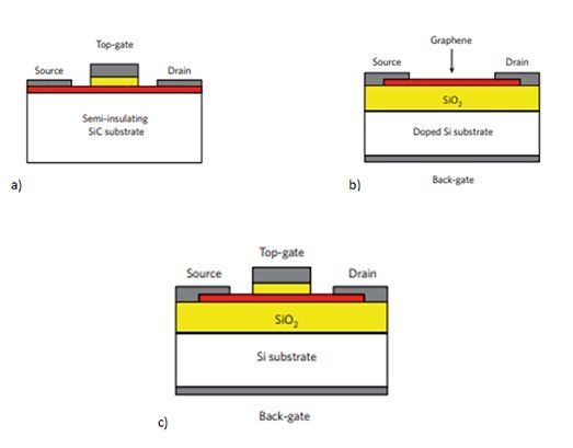
What Is a Graphene Field Effect Transistor (#GFET)?


from Twitter https://twitter.com/wladek60

November 16, 2020 at 10:21AM
via IFTTT

Nov 13, 2020

Digi-Key releases 1.5 million SnapEDA #CAD #models https://t.co/IzCT3WnWTC #semi https://t.co/BBXV146WQ7


from Twitter https://twitter.com/wladek60

November 13, 2020 at 07:47PM
via IFTTT

RT @gvanrossum: I decided that retirement was boring and have joined the Developer Division at Microsoft. To do what? Too many options to say! But it’ll make using Python better for sure (and not just on Windows :-). There’s lots of open source here. Watch this space. . #semi https://t.co/kJI0LT4jUA


from Twitter https://twitter.com/wladek60

November 13, 2020 at 07:35PM
via IFTTT

Nov 12, 2020

Fwd: Elena Gnani DL - Tunnel FETs: Device Physics and Realizations

To view complete details for this event, click here to view the announcement

Elena Gnani DL - Tunnel FETs: Device Physics and Realizations


The EDS Germany Chapter and NanoP proudly presents Elena Gnani from University of Bologna, Bologna, Italy for a Distinguished Lecture on "Tunnel FETs: Device Physics and Realizations". The lecture will be held on 18th January 2021 at 3pm Berlin time.

Date and Time

Location

The Distiguished Lecture will be held via Zoom. Login information provided before the event and requires registration.

Hosts

Registration

  • Starts 12 November 2020 04:30 PM
  • Ends 16 January 2021 05:00 PM
  • All times are Europe/Berlin
  • No Admission Charge

Nov 10, 2020

[mos-ak] [2nd Announcement and C4P] 13th Virtual MOS-AK Workshop, Silicon Valley, Dec. 10-11 2020


Together with  local organization team, International MOS-AK Board of R&D Advisers as well as all the Extended MOS-AK TPC Committee, we have the pleasure to invite to consecutive, 13th International MOS-AK Workshop which will be organized as the virtual/online event on Dec. 10-11, 2020 (preceding the IEDM and Q4 CMC Meetings)

Planned virtual 13th International MOS-AK Workshop aims to strengthen a network and discussion forum among experts in the field, enhance open platform for information exchange related to compact/SPICE modeling and Verilog-A standardization, bring academic and industrial experts in the compact modeling field together, as well as obtain feedback from technology developers, circuit designers, and CAD/EDA tool developers and vendors. 

Venue: Virtual/Online

Online Workshop Registration to be open 
(any related enquiries can be sent to registration@mos-ak.org)

Topics to be covered include the following among other related to the compact/SPICE modeling and its Verilog-A standardization:
  • Compact Modeling (CM) of the electron devices
  • Advances in semiconductor technologies and processing
  • Verilog-A language for CM standardization
  • New CM techniques and extraction software
  • Open Source (FOSS) TCAD/EDA modeling and simulation
  • CM of passive, active, sensors and actuators
  • Emerging Devices, TFT, CMOS and SOI-based memory cells
  • Microwave, RF device modeling, high voltage device modeling
  • Nanoscale CMOS, BiCMOS, SiGe, GaN, InP devices and circuits
  • Technology R&D, DFY, DFT and reliability/ageing IC designs
  • Foundry/Fabless Interface Strategies
Important Dates: 
  • 2nd Announcement: Nov. 2020
  • Final Workshop Program: Dec. 2020
  • Virtual MOS-AK Workshop: Dec. 10-11, 2020
Online Abstract Submission to be open 
(any related enquiries can be sent to abstbstracts@mos-ak.org)

WG10112020

--
You received this message because you are subscribed to the Google Groups "mos-ak" group.
To unsubscribe from this group and stop receiving emails from it, send an email to mos-ak+unsubscribe@googlegroups.com.
To view this discussion on the web visit https://groups.google.com/d/msgid/mos-ak/891cd84d-b714-44b6-85af-4e361a257515n%40googlegroups.com.

[mos-ak] [online publications] Virtual MOS-AK Workshops (Sept. 2020)

Arbeitskreis Modellierung von Systemen und Parameterextraktion 
Modeling of Systems and Parameter Extraction Working Group
Virtual MOS-AK Workshops (Sept. 2020)

Local organization teams together with the International MOS-AK Board of R&D Advisers as well as all the Extended MOS-AK TPC Committee have organized two subsequent virtual/online workshops
  • MOS-AK Workshop as ESSDERC/ESSCIRC Virtual Educational Event
    • http://www.mos-ak.org/grenoble_2020/
    • Sept.15, 2020 (16:00 - 17:00 CET with livestreaming) 
  • MOS-AK Workshop at THM Giessen (D),
    • http://www.mos-ak.org/giessen_2020/
    • Tue 29.09.2020 - MOS-AK
    • Wed 30.09.2020 - MOS-AK & IEEE EDS MQ
    • Thu 01.10.2020 - IEEE EDS MQ & SB MOS Symposium
Online Publications:
There are MOS-AK technical presentations covering selected aspects of the compact/SPICE modeling and its Verilog-A standardization (see  the slide presentations online at respective corresponding links).

Postworkshop Publications:
Selected best MOS-AK technical presentation will be recommended for further publication in a special Solid State Electronics issue on compact modeling planned for 2021

The MOS-AK Association plans to continue its standardization efforts by organizing future compact modeling meetings, workshops and courses around the globe thru 2020 and next 2021 year, including:
  • Virtual MOS-AK Silicon Valley (US), Dec. 10-11 2020 
  • FOSDEM CAD/EDA DevRoom, ULB, (B) Feb. 2021
  • MOS-AK at LAEDC (MX),  April 18-20 2021
  • FOSS TCAD/EDA at 5NANO2021, Kottayam (IN) April 2021
  • MIXDES CM Session, Wroclaw (PL), June 2021
    with IEEE EDS MQ
  • 5th Sino MOS-AK Xi'an (CN), July  2021
  • 19th MOS-AK at ESSDERC/ESSCIRC, Grenoble (F) Sept. 2021
  • 14th US MOS-AK Workshop, Silicon Valley (US) Dec. 2021
    in timeframe of IEDM and Q4 CMC Meetings
W.Grabinski on the behalf of International MOS-AK Committee  

WG10112020

--
You received this message because you are subscribed to the Google Groups "mos-ak" group.
To unsubscribe from this group and stop receiving emails from it, send an email to mos-ak+unsubscribe@googlegroups.com.
To view this discussion on the web visit https://groups.google.com/d/msgid/mos-ak/d9894925-c3fa-4c0c-8a23-4a6ca27323a3n%40googlegroups.com.

Software Freedom in Europe


from Twitter https://twitter.com/wladek60

November 10, 2020 at 02:29PM
via IFTTT

Nov 5, 2020

[paper] TFT for Mixed Signal and Analog Computation

Eva Bestelink, Olivier de Sagazan, Lea Motte, Max Bateson, Benedikt Schultes, S. Ravi P. Silva,
and Radu A. Sporea
Versatile Thin‐Film Transistor with Independent Control of Charge Injection and Transport
for Mixed Signal and Analog Computation
Adv. Intell. Syst.. (2020) pp.1-9, DOI:10.1002/aisy.202000199 

Abstract: New materials and optimized fabrication techniques have led to steady evolution in large area electronics, yet significant advances come only with new approaches to fundamental device design. The multimodal thin-film transistor introduced here offers broad functionality resulting from separate control of charge injection and transport, essentially using distinct regions of the active material layer for two complementary device functions, and is material agnostic. The initial implementation uses mature processes to focus on the device’s fundamental benefits. A tenfold increase in switching speed, linear input–output dependence, and tolerance to process variations enable low-distortion amplifiers and signal converters with reduced complexity. Floating gate designs eliminate deleterious drain voltage coupling for superior analog memory or computing. This versatile device introduces major new opportunities for thin-film technologies, including compact circuits for integrated processing at the edge and energy-efficient analog computation.

Figure: Outcomes of separating control for injection and conduction shown via TCAD simulation. a) MMT transient response is much faster than conventional contact-controlled TFTs
b) A MMT with multiple, appropriately sized CG1 gates can function as a digital-to-analog converter (DAC) with CG2 providing an enabling, sampleand-hold (S/H) function. 

Acknowledgements: E.B. and R.A.S. contributed equally to this work. This work was partly supported through EPSRC grants EP/R511791/1 and EP/R028559/1 and Research Fellowship 10216/110 from the Royal Academy of Engineering of Great Britain. Device fabrication had been performed on the NanoRennes platform. The authors thank Dr. Brice Le Borgne for initial liaison and process discussions, Prof. John M. Shannon for on-going advisory meetings, Prof. Craig Underwood for reviewing the manuscript, Dr. David Cox and Mr. Mateus Gallucci Masteghin for assistance with the SEM images.

Nov 4, 2020

IEEE Germany EDS Chapter Elections

The IEEE Germany EDS Chapter has elected new ExCom members for the term 2020/2021. An exciting new leadership team has been built to establish EDS activities in Germany.

The new ExCom:
  • Chair: Mike Schwarz (TH Mittelhessen)
  • Vice Chair: Joachim Burghartz (Universität Stuttgart, IMS Chips)
  • Treasurer: Manfred Berroth (Universität Stuttgart)
  • Secretary: Sevda Abadpour (Karlsruhe Institute of Technology)
Further information is available online https://r8.ieee.org/germany-eds