Nov 21, 2023

[webinar] Open Source Silicon Landscape

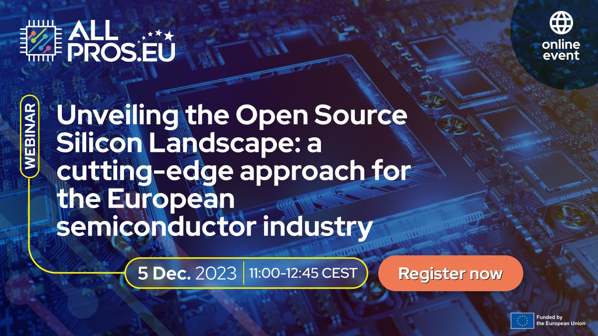
Unveiling the Open Source Silicon Landscape
a cutting-edge approach for the European semiconductor industry
5 December 2023


Who should attend and why:
  • Policymakers at the regional, national, and European level who want to strengthen their respective semiconductor ecosystem while collaborating and contributing to the Union’s industry as a whole
  • Research and academia representatives who are interested in deepening their knowledge or discovering the potential of the Open Source Silicon landscape
  • SMEs in the semiconductor industry who aim to expand and innovate their business by using a cutting-edge approach
  • Start-ups that are eager to elevate their business to the next level by embracing vanguard strategies
  • Citizen scientists and the general public who would like to have a better understanding of the new horizons in the semiconductor landscape
  • Experts active in industrial development who are interested in integrating potential new approaches
Registration:

The event is free of charge, but registration is mandatory. Registrants will receive the link to access the event by email.

Agenda:

11:00 - 11:05 Welcome
11:05 - 11:10 Introducing Open Source Silicon
11:10 - 11:20 BACKGROUND Open source silicon between software and hardware Background
11:20 - 11:40 POLICY BRIEF PRESENTATION Open source silicon’s position in the semiconductor value chain
11:40 - 12:35 PANEL Key opportunities and threats relevant to open source silicon strategies
12:35 - 12:45 Q&A and conclusions

Nov 20, 2023

[C4P] LAEDC 2024

CALL FOR PAPERS & POSTERS


LAEDC 2024 R&D topics of interest include, but are not limited to:
  • All electron-based devices
  • Electron Devices for Quantum Computing
  • RF-MMW-5G
  • Semiconductor-, MEMS- and Nanotechnologies
  • Packaging, 3D integration
  • Sensors and actuators
  • Display technology
  • Modeling and simulation
  • Reliability and yield
  • Device characterization
  • Reliability
  • Agrivoltaics

  • Flexible electronics
  • Biomedical Devices
  • Circuit-device interaction
  • Novel materials and process modules
  • Technology roadmaps
  • Electron device engineering education
  • Electron device outreach
  • Optoelectronics, photovoltaic and photonic devices and systems
  • Humanitarian Projects
  • STEM Initiatives
  • Energy harvesting
  • 2D Materials and Devices
IMPORTANT DATES:
  • Paper submission deadline: January 15, February 19, 2024
  • Author notification: April 1, 2024
  • LAEDC Conference Dates: MAY 8-10 2024
SPECIAL SESSIONS:
  • MOS-AK Workshop
  • IEEE EDS MQ
  • LAEDC Summer School
  • IEEE WIE/YP Session
  • Humanitarian Technology Session
ABOUT GUATEMALA:
Guatemala, country of Central America. The dominance of an Indigenous culture within its interior uplands distinguishes Guatemala from its Central American neighbours. The origin of the name Guatemala is Indigenous, but its derivation and meaning are undetermined. Some hold that the original form was Quauhtemallan (indicating an Aztec rather than a Mayan origin), meaning “land of trees,” and others hold that it is derived from Guhatezmalha, meaning “mountain of vomiting water” - referring no doubt to such volcanic eruptions as the one that destroyed Santiago de los Caballeros de Guatemala (now Antigua Guatemala), the first permanent Spanish capital of the region’s captaincy general. The country’s contemporary capital, Guatemala City, is a major metropolitan centre. Quetzaltenango, in the western highlands, is the nucleus of the Indigenous population.


Nov 16, 2023

Chipsalliance Technology Update - Nov. 2023

November 9, 2023

Check out the presentations below, and watch the replay here

  • Project Open Se Cura (slides)
    Kenny Vassigh, Bangfei Pan, Cindy Liu, Kai Yick, Google, Michael Gielda, Antmicro, Brian Murray, Verisilicon
  • Caliptra Workgroup Update (slides)
    Andres Lagar-Cavilla, Google
  • Enabling UVM testbenches in Verilator (slides)
    Michael Gielda, Karol Gugala, Antmicro
  • FuseSOC: Package manager and build abstraction tool for FPGA/ASIC development (slides)
    Olof Kindgren, Qamcom
  • CHIPYard: An Open Source RISC-V Design Framework (slides)
    Sagar Karandikar, U.C. Berkeley

Watch the Replay

Nov 14, 2023

[paper] Boropheneand Metal Interface

Vaishnavi Vishnubhotla, Sanchali Mitra, and Santanu Mahapatraa
First-principles based study of 8-Pmmn boropheneand metal interface
J. Appl. Phys. 134, 034301 (2023); doi: 10.1063/5.0144328
DOI 10.1063/5.0144328

Nano-Scale Device Research Laboratory, Department of Electronic Systems Engineering, 
Indian Institute of Science (IISc) Bangalore, India

Abstract: Borophene, the lightest member of mono-elemental 2D materials family, has attracted much attention due to its intriguing polymorphism. Among many polymorphs, digitally discovered 8-Pmmn stands out owing to its unique tilted-Dirac fermions. However, the property of interfaces between 8-Pmmn and metal substrates has so far remained unexplored, which has critical importance of its application in any electronic devices. Here, with the help of density functional theory, we show that the unique tilted-Dirac property is completely lost when 8-Pmmn borophene is interfaced with common electrode materials such as Au, Ag, and Ti. This is attributed to the high chemical reactivity of borophene as observed from crystal orbital Hamilton population and electron localization function analysis. In an effort to restore the Dirac property, we insert a graphene/hexagonal-boron-nitride (hBN) layer between 8-Pmmn and metal, a technique used in recent experiments for other 2D materials. We show that while the insertion of graphene successfully restores the Dirac nature for all three metals, hBN fails to do so while interfacing with Ti. The quantum chemical insights presented in this work may aid in to access the Dirac properties of 8-Pmmn in experiments.
FIG: (a) Top and side views of 3 × 3 × 1 supercell of 8-Pmmn borophene. The lattice parameters are a = 3.26 Å, b = 4.52 Å, and h = 2.19 Å. The inner and ridge atoms are denoted by blue and green atoms, respectively. (b) Crystal orbital Hamilton population (COHP) analysis and (c) electron localization function (ELF) plot for graphene and 8-Pmmn borophene.

Acknowledgments: The authors acknowledge the Supercomputer Education and Research Center (SERC), Indian Institute of Science (IISc), Bangalore, for CPU- and GPU-based computations. The computational charges were aided by the Mathematical Research Impact Centric Support (MATRICS) scheme of Science and Engineering Research Board (SERB), Government of India, under Grant No. MTR/2019/000047.

Nov 13, 2023

[paper] PSP RF Model

Xiaonian Liu1, 2 and Yansen Liu1
A Scalable PSP RF Model for 0.11 µm MOSFETs
Progress In Electromagnetics Research Letters, Vol. 113, 43–51, 2023
DOI :10.2528/PIERL23081405

1 School of Physics and Electronics, Hunan Normal University, Changsha 410081, China.
2 Key Laboratory of Physics and Devices in Post-Moore Era, College of Hunan Province, Changsha 410081, China.


Abstract : An accurate, efficient and scalable SPICE model is essential for modern integrated circuits design, especially for radio frequency (RF) circuit design. A PSP based scalable RF model is extracted and verified in 0.11 CMOS manufacturing process. The S parameter measurement system and open-short de-embedding technique is applied. The macro-model equivalent subcircuit and parameters extraction strategy are discussed. The extracted model can match the de-embedded S parameters data well. By combining the model parameters’ dependencies on each geometry quantity, the scalable expression of parameters with all geometry quantities included can be obtained. This work can be a reference for the RF MOSFETs modeling and RF circuit design.

Fig: The RF PSP Model Subcircuit

Acknowledgment : This work is supported by the National Natural Science Foundation of China under Grant 62204083, and the Youth Fund of Education Department of Hunan Province under Grant 21B0057.