Aug 31, 2020

[JICS] SBMicro2020 Special Section Issue

Journal of Integrated Circuits and Systems
SBMicro2020 Special Section Issue
Vol 15 No 2 (2020)

The Journal of Integrated Circuits and Systems is an effort of both Brazilian Microelectronics Society - SBMicro and Brazilian Computer Society - SBC to create a new scientific journal covering intended to present state-of-art papers on Integrated Circuits and Systems, covering the fields of Process and Materials, Device and Characterization, Design, Test and CAD, among other relevant topics. The JICS is indexed in Scopus and Scimagojr.

SBMicro2020 Special Section Guest Editors:
Durga Misra, New Jersey Institute of Technology – NJIT, United States
Michelly de Souza, Centro Universitário FEI, Brazil

Online ISSN: 1872-0234 (from 2017 on)
Printed ISSN: 1807-1953 (prior to 2017)
Published: 2020-08-23


[paper] Bulk CMOS Technology at Sub-Kelvin Temperature

Characterization and Modeling of 0.18µm Bulk CMOS Technology 
at Sub-Kelvin Temperature 
Teng-Teng Lu1,2, Zhen Li1,2, Chao Luo1,2, Jun Xu2, Weicheng Kong3
and Guoping Guo1 (Member, IEEE) 
IEEE J-EDS, vol. 8, pp. 897-904, 2020
DOI: 10.1109/JEDS.2020.3015265.

1Key Laboratory of Quantum Information, University of Science and Technology of China, Hefei 230026, China 
2Department of Physics, University of Science and Technology of China, Hefei 230026, China 
3Department of Quantum Hardware, Origin Quantum Computing Company Limited, Hefei 230026, China

Abstract: Previous cryogenic electronics studies are mostly at 77K and 4.2K. Cryogenic characterization of a 0.18μm standard bulk CMOS technology (operating voltages: 1.8V and 5V) is presented in this paper. Several NMOS and PMOS devices with different width to length ratios (W/L) were extensively tested and characterized under various bias conditions at sub-kelvin temperature. In addition to devices dc characteristics, the kink effect and current overshoot phenomenon are observed and discussed at sub-kelvin temperature. Especially, the current overshoot phenomenon in PMOS devices at sub-kelvin temperature is shown for the first time. The transfer characteristics of MOSFET devices (1.8V W/L = 10μm/10μm) at sub-kelvin temperature are modeled using the simplified EKV model. This work facilitates the CMOS circuits design and the integration of CMOS circuits with silicon-based quantum chips at extremely low temperatures.
FIG: IDS-VGS curves of large thin TOX NMOS (a,b,e,f) and PMOS (c,d,g,h) devices at sub-kelvin temperature measured (symbols) and simulated (solid lines). 

Aknowlegement: This work was supported in part by the National Key Research and Development Program of China under Grant 2016YFA0301700, in part by the National Natural Science Foundation of China under Grant 11625419, in part by the Anhui initiative in Quantum information Technologies under Grant AHY080000, and in part by the USTC Center for Micro and Nanoscale Research and Fabrication.

[paper] Monolithic Pixel Detector in SOI Technology

High spatial resolution monolithic pixel detector in SOI technology 
R. Bugiela1, S. Bugiela2, D. Dannheimb, A. Fiergolskib, D. Hyndsb,3, M. Idzika, P. Kapustac, M. Munkerb, A. Nurnbergb4, S. Spannagelb,5, K. Swienteka, W. Kucewicza
aAGH-UST, Poland, bCERN, Switzerland, cIFJ PAN, Poland
CLICdp-Pub-2020-004
06 August 2020

1Present: CNRS/IPHC, France.
2Present: CNRS/IPHC, France.
3Present: NIKHEF, Amsterdam, Netherlands.
4Present: KIT, Karlsruhe, Germany.
5Present: DESY, Hamburg, Germany.

Abstract: This paper presents test-beam results of monolithic pixel detector prototypes fabricated in 200nm Silicon-On-Insulator (SOI) CMOS technology studied in the context of high spatial resolution performance. The tested detectors were fabricated on a 500µm thick highresistivity Floating Zone type n (FZ-n) wafer and on a 300 µm Double SOI Czochralski type p (DSOI Cz-p) wafer. The pixel size is 30µm×30µm and two different front-end electronics architectures were tested, a source follower and a charge-sensitive preamplifier. The test-beam data analyses were focused mainly on determination of the spatial resolution and the hit detection efficiency. In this work different cluster formation and position reconstruction methods are studied. In particular, a generalization of the standard η-correction adapted for arbitrary cluster sizes, is introduced. The obtained results give in the best case a spatial resolution of about 1.5µm for the FZ-n wafer and about 3.0µm for the DSOI Cz-p wafer, both detectors showing detection efficiency above 99.5%.

Fig.: Simplified schematics of Silicon-On-Insulator structures. The Buried N(P)-Well (BN(P)W) is a layer dedicated to shielding the electronics from the sensors electric field.

Aknowlegement: This work was financed by the European Union Horizon 2020 Marie Sklodowska-Curie Research and Innovation Staff Exchange program under Grant Agreement no. 645479 (E-JADE) and also by the Polish Ministry of Science and Higher Education from funds for science in the years 2017 – 2018 allocated to an international co-financed project. The authors would like to thank also the operators of the CERN SPS beam line and North Area test facilities.

Opinion Can Israel lead the #opensource code revolution? The Israeli tech scene is based on partnerships, innovation and independent thinking which are all vital in open-source code https://t.co/GdyYArG2sa https://t.co/yG6MPmp7bG


from Twitter https://twitter.com/wladek60

August 31, 2020 at 10:31AM
via IFTTT

Aug 28, 2020

TSMC: All the Processes, All the Fabs

TSMC Technology Symposium: All the Processes, All the Fabs
by Paul McLellan at breakfast-bytes
27 Aug 2020

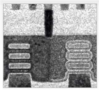
TSMC has new transistor structure (nanosheet) and new materials such as high mobility channel, 2D, carbon nanotube (CNT). TSMC has already demonstrated at 32Mb nanosheet SRAM fully-functional at 0.46V. It has also identified promising 2D materials such as MoS2 (molybdenum disulfide). At IEDM last year, they disclosed the first BEOL CNT power-gating device integrated with silicon-based CMOS.
Scaling continues with EUV advances with the current generation of scanners. They are also working with ASML (the only supplier of EUV equipment) on High-NA EUV [read more...]