Jun 17, 2015

3rd Training Course on Compact Modeling

 3rd TCCM, 
 organized as IEEE EDS Mini-Colloquium 
 (http://eds.ieee.org/lectures.html?eid=136)

Co-organizer: Institute of Electron Technology, Warsaw, Poland
Technical Program Promoter: DMCS, Lodz University of Technology, Łódź, Poland

Date: June 24, 2015.
Place: Hotel Bulwar (Lejda room) ul. Bulwar Filadelfijski 18, 87-100 Toruń, Poland
www: http://www.hotelbulwar.pl

Final schedule of TCCM:
9:00 Wladek Grabinski, Opening
9:10 Henryk Przewłocki, "Weaknesses and corrections of the classical theory of photoelectric phenomena in the MOS system"
10:00 Juin J.Liou, "Compact Modeling of Junction Failure in Semiconductor Devices Subject to Electrostatic Discharge Stresses"
10:50 Coffee break
11:10 Jean-Michel Sallese, "Modeling Junctionless Field Effect Transistors"
12:00 Mike Brinson, "A unified approach to compact device modelling with the open source packages Qucs/ADMS and MAPP/Octave"
13:00 Lunch
14:30 Benjamin Iniguez, "Physically-Based Compact Modeling of GaN HEMT"
15:20 Wladek Grabinski, "Verilog-A Compact Model Standardization"
16:10 Daniel Tomaszewski, "Compact modeling and statistical modeling for parametric yield improvement"
17:00 Wladek Grabinski, Closing

Jun 12, 2015

Micro&Nano 2015 - 2nd Announcement

6th Micro & Nano Conference on Micro - Nanoelectronics, Nanotechnologies and MEMs
4-7 October, 2015, Athens, Greece

http://conference-micronano2015.micro-nano.gr
Second Announcement

The "Micro&Nano 2015" Conference will be held at the Fenix Hotel, in Glyfada, Athens, Greece. The Best Western Hotel Fenix is conveniently located in Glyfada, an attractive resort in the south coast of Athens. More details on the Conference venue can be found on the conference website:
<http://conference-micronano2015.micro-nano.gr>

Conference Topics:
  • Micro and Nano- Fabrication
  • Materials for Electronics, Photonics and Sensors
  • Electronic, Optoelectronic and Photonic Devices
  • Sensors and Actuators
All abstracts should not exceed the limit of 300 words. Please follow the abstract template that can be found here. The deadline for abstract submission is on 30 June 2015.

The Conference abstracts will be published in the "Abstract Book" that will be distributed to all the participants, at the beginning of the Conference. Selected papers will be published, after peer-review, in special issues of the following international journals:
  • Nanoscale Research Letters (the nanoscience related articles)
  • Microelectronic Engineering
[read more: http://conference-micronano2015.micro-nano.gr]

May 15, 2015

[mos-ak] [2nd Announcement and Call for Papers] Autumn 2015 MOS-AK Workshop at ESSDERC/ESSCIRC

 Autumn 2015 MOS-AK Workshop at ESSDERC/ESSCIRC
Graz (A) September 18, 2015
2nd Announcement and Call for Papers

Together with the MOS-AK Workshop Scientific Program Coordinators Larry Nagel and Andrei Vladimirescu, local workshop chairs Benjamin Iniguez, URV (SP) and Jean-Michel Sallese, EPFL (CH) as well as Extended MOS-AK TPC Committee, we have pleasure to invite to the MOS-AK Workshop which will be held in Graz (A) at the ESSDERC/ESSCIRC Conference where also a joint modeling session (invited talks by Prof. C.C.Enz and Prof. C.Hu) as well as a session with regular modeling paper (and the invited talk by Prof. M.Lundstrom) are planed. Following MOS-AK workshop is organized with aims to strengthen a network and discussion forum among experts in the field, enhance open platform for information exchange related to compact/SPICE modeling and Verilog-A standardization, bring people in the compact modeling field together, as well as obtain feedback from technology developers, circuit designers, and CAD/EDA tool developers and vendors.

Venue:   
University of Technology,
Campus Inffeldgasse
Graz (A)

Important Dates:
  • Call for Papers - March 2015
  • 2nd Announcement - May 2015
  • Final Workshop Program - July 2015
  • MOS-AK Workshop - Sept.18, 2015
    • 08:30 - 09:00 - On-site Registration
    • 09:00 - 10:30 - Morning MOS-AK Session
    • 11:00 - 12:00 - CM Standardization Pannel
    • 12:00 - 13:00 - Lunch
    • 13:00 - 16:00 - Afternoon MOS-AK Session
Topics to be covered include the following:
  • Advances in semiconductor technologies and processing
  • Compact Modeling (CM) of the electron devices
  • Verilog-A language for CM standardization
  • New CM techniques and extraction software
  • Open Source TCAD/EDA modeling and simulation
  • CM of passive, active, sensors and actuators
  • Emerging Devices, CMOS and SOI-based memory cells
  • Microwave, RF device modeling, high voltage device modeling
  • Nanoscale CMOS devices and circuits
  • Technology R&D, DFY, DFT and IC Designs
  • Foundry/Fabless Interface Strategies
Online Abstract Submission:
Authors should submit an abstract using on-line MOS-AK submission form
(any related inquiries can be sent to abstracts@mos-ak.org)
http://www.mos-ak.org/graz_2015/abstracts.php

Free online workshop registration:
(any related inquiries can be sent to register@mos-ak.org)
http://www.mos-ak.org/graz2015/registration.php

Postworkshop publications:
Selected best MOS-AK technical presentation will be recommended for further publication in a special issue of the International Journal of High Speed Electronics and Systems

Extended MOS-AK Committee

WG052015

--
You received this message because you are subscribed to the Google Groups "mos-ak" group.
To unsubscribe from this group and stop receiving emails from it, send an email to mos-ak+unsubscribe@googlegroups.com.
To post to this group, send email to mos-ak@googlegroups.com.
Visit this group at http://groups.google.com/group/mos-ak.
For more options, visit https://groups.google.com/d/optout.

Mar 16, 2015

[MOS-AK/DATE 2015 Workshop] CEA-Leti's predictive model takes FDSOI further

 CEA-Leti's predictive model takes FDSOI further 

During DATE 2015’s MOS-AK Workshop, CEA-Leti presented the newest version of its advanced compact model for ultra-thin body and buried oxide fully depleted SOI (UTBB-FDSOI) technology.

Fully Depleted Silicon On Insulator (FDSOI) is a planar process technology that relies on two primary innovations. First, an ultra-thin layer of insulator, called the buried oxide, is positioned on top of the base silicon.

Then, a very thin silicon film implements the transistor channel. Thanks to its thinness, there is no need to dope the channel, thus making the transistor fully depleted. The combination of these two innovations is called “ultra-thin body and buried oxide Fully Depleted SOI” or UTBB-FDSOI.

Back in 2013, CEA-Leti had deployed a first compact model, but working in close cooperation with STMicroelectronics, the research lab understood that more subtle back gate channelling effects had to be addressed to fully exploit the benefits of UTBB-FDSOI and to explore the transistors’ behaviour in more details.

New analytical equations were written from scratch for the Leti-UTSOI2.1 compact model, improving on the predictability and accuracy capabilities of the previous version, Leti-UTSOI2.

To date, other models from the University of Hiroshima, and from the University of Berkeley fail to account for inversion effects at the back interface, when a strong forward back bias (FBB) is applied, told us Thierry Poiroux, Leti research engineer and model co-developer.

More specifically, the French lab used a unique analytical resolution scheme for the calculation of surface potentials at both interfaces of the transistor body, offering a refined description of narrow-channel effects, with an improved accuracy of moderate inversion regime and gate tunnelling current modelling.

Because the model is analytical, it is much faster than any numerical simulation. It is now available in all major SPICE and Fast SPICE simulators through licences with EDA vendors and will allow fabless companies and IC designers to virtually explore different UTBB-FDSOI parameters within a given foundry process node. The new model can also be used by foundries and fabless companies to perform a predictive analysis of future nodes to come, in order to orient their ongoing process optimization.

for more information visit CEA-Leti at www.leti.fr

Mar 8, 2015

[BOOK] FinFET Modeling for IC Simulation and Design Using the BSIM-CMG Standard

 FinFET Modeling for IC Simulation and Design Using the BSIM-CMG Standard
 Yogesh Singh Chauhan, Darsen Lu, Sriramkumar Venugopalan, Sourabh Khandelwal, Juan Pablo Duarte, Navid Paydavosi, Ai Niknejad, Chenming Hu

DESCRIPTIONThis book is the first to explain FinFET modeling for IC simulation and the industry standard – BSIM-CMG - describing the rush in demand for advancing the technology from planar to 3D architecture, as now enabled by the approved industry standard. The book gives a strong foundation on the physics and operation of FinFET, details aspects of the BSIM-CMG model such as surface potential, charge and current calculations, and includes a dedicated chapter on parameter extraction procedures, providing a step-by-step approach for the efficient extraction of model parameters.

KEY FEATURES
  • Learn how to do FinFET modeling using the BSIM-CMG standard from the experts
  • Authored by the lead inventor and developer of FinFET, and developers of the BSIM-CMG standard model, providing an experts’ insight into the specifications of the standard
  • The first book on the industry-standard FinFET model - BSIM-CMG
With this book you will learn:
  • Why you should use FinFET
  • The physics and operation of FinFET
  • Details of the FinFET standard model (BSIM-CMG)
  • Parameter extraction in BSIM-CMG
  • FinFET circuit design and simulation
READ MORE:
​http://store.elsevier.com/product.jsp?isbn=9780124200319
http://www.amazon.com/FinFET-Modeling-IC-Simulation-Design/dp/0124200311
http://www.amazon.in/FinFET-Modeling-IC-Simulation-Design/dp/0124200311

Feb 17, 2015

MIXDES 2015, June 25-27, 2015; Torun, Poland

 22nd International Conference "Mixed Design of Integrated Circuits and Systems"
 MIXDES 2015, June 25-27, 2015; Torun, Poland

The deadline for regular paper submission is approaching (March 2nd, 2015). If you are going to contribute, I encourage you to register your papers as soon as possible. You will be able to update the paper details and the document file at any time till the final paper version deadline (May 15th, 2015). The early submission will allow us to take care of your paper just now, especially start the reviewer assignments and begin the formatting verification process.

[read more...]

Feb 16, 2015

Call for Papers [dvconeurope] DVCon-Europe 2015

 DVCON EUROPE 2015
The Design and Verification Conference & Exhibition Europe (DVCon Europe) is the premier conference for system architects, concept engineers, software developers, design and verification engineers, and IP integrators to share the latest methodologies and technologies on the practical use of EDA and IP languages and standards used in electronic design.

The focus of this highly technical conference is on the industrial application of specialized design and verification languages such as SystemC, SystemVerilog, VHDL, UVM or e; assertions in SVA or PSL; the use of AMS languages; design automation using IP-XACT; and the use of general purpose languages C and C++.

CALL FOR PAPERS
This call for papers solicits presentations that are highly technical and reflect real life experiences in using EDA languages, standards, methodologies and tools. Industry applications of interest include (but are not limited to) automotive, mobile communication, aerospace, healthcare, chip-cards, consumer and power electronics. Submissions are encouraged in (but not restricted to) the four topic areas listed below. Low power techniques and design for functional safety (e.g., ISO 26262, DO-254) are pervasive and can be addressed in any of these topics areas.

Please submit your draft version of the paper by May 1, 2015. Detailed instructions on the paper requirements and submission process can be found on www.dvcon-europe.org

ESSCIRC/ESSDERC 2015 website is now active

 ESSCIRC/ESSDERC 2015 website is now active: www.esscirc-essderc2015.org

 The deadline for paper submission is 2 April, 2015.
 Looking forward to seeing you in Graz!

Prof. Wolfgang Pribyl: General Chair ESSCIRC/ESSDERC 2015
Franz Dielacher, Gernot Hueber: ESSCIRC TPC Chairs
Martin Schrems, Tibor Grasser: ESSDERC TPC Chairs

Feb 12, 2015

Call for Papers: [fdl7] FDL2015

 Forum on Specification & Design Languages
 [fdl7] FDL 2015 CALL FOR PAPERS
  September 14-16, 2015 | Barcelona, Spain

FDL is an international forum to exchange experiences and promote new trends in the application of languages, their associated design methods and tools for the design of electronic systems. FDL stimulates scientific and controversial discussions within and in-between scientific topics as described below. The program structure includes research working sessions, embedded tutorials, panels, and technical discussions. The Forum includes tutorials and fringe meetings, such as user group or standardization meetings. “Wild and Crazy Ideas” are also welcome.

Important Dates:

  • Proposals for Special Session: March 22, 2015
  • Full Research Paper submission: May 4, 2015
  • Other Contributions submission: June 10, 2015
  • Notification of acceptance: July 4, 2015
  • Camera ready papers: August 12, 2015


[1st announcement] #SIXHackathon 20-21 March 2015 in Zurich (CH)

 #SIXHackathon 20-21 March 2015 in Zurich (CH)
 [1st announcement] 

Are you interested in the financial technology sector (FinTech)? Are you on the lookout for a challenge? Then take part in SIX's Hackathon in Zurich 20 - 21 March 2015 and rub shoulders with one of the financial sector's leading IT companies for 30 hours.

What you can expect
Fun, challenging questions, exciting data sets, new ideas, networking opportunities, an exchange with like-minded people; people interested in FinTech and employees from SIX who are also participating.

What you have to do
SIX will provide you with data and APIs (interface information) from FinTech. You will work in small teams. The aim is to present an expert jury with a prototype or a concept after 30 hours. You can either select a topic freely or take inspiration from one of the workshops on big data in the financial technology sector and payment solutions. You will be competing against around 100 participants.

Who is eligible to take part
In principle, any student aged over 18 at a Swiss university or university of applied science and all SIX employees are eligible to take part. Participants must have an affinity and a relevant skill-set in the areas of software development, graphic or interface design, marketing, project management or similar.

Why it’s worth to participate
You will have the opportunity to prove your skills using real-life problems and present your ideas to an expert jury. Furthermore, SIX is searching for new talents – depending on your background, successful Hackathon participants could be offered a permanent position or a traineeship at SIX.

FOR MORE INFORMATION:
http://www.six-group.com/careers/en/site/hackathon.html
REGISTER NOW:
http://www.six-group.com/careers/en/site/hackathon/registration.html

Feb 10, 2015

Call for Papers: ESSCIRC/ESSDERC 2015 Graz (A)

the 41st ESSCIRC and 45th ESSDERC Conferences will take place on 14 to 18 September 2015 in Graz, Austria. The event is technically co-sponsored by the IEEE Electron Device Support and the IEEE Solid-State Circuit Society.

Detailed information about the conference will soon be provided at the ESSCIRC/ESSDERC 2015 website:
www.esscirc-essderc2015.org

The deadline for paper submission is 2 April, 2015

[read more...]

Feb 2, 2015

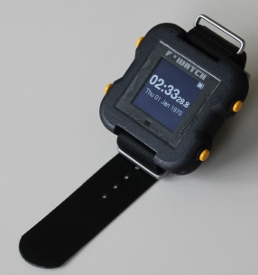
FOSS GPS watch

F*watch! Why should your watch be different?

(FOSS) F*watch is an infinitely hackable GPS watch with many sensors based on a 100% Free design. Everything is free, from the PCB and watch housing design to the software stack. Moreover, only free software FOSS tools have been used during the development.

The FOSDEM2015 talk described the development process and shows a first prototype, along with performance measurements and future plans.

FOSDEM2015 Speakers:


Links: F*Watch wiki


Jan 22, 2015

[mos-ak] [Announcement and Call for Papers] Spring 2015 MOS-AK Workshop at DATE

 Spring 2015 MOS-AK Workshop at DATE
  Grenoble March 12, 2015
  Announcement and Call for Papers 
 
 Together with the MOS-AK Workshop Scientific Program Coordinators Larry Nagel and Andrei Vladimirescu, local workshop chairs Patrick Martin, CEA (F) and Benjamin Iniguez, URV (SP) as well as Extended MOS-AK TPC Committee, we have pleasure to invite to the Spring MOS-AK Workshop which will be held in Grenoble (F) at the DATE Conference. The event is organized with aims to strengthen a network and discussion forum among experts in the field, enhance open platform for information exchange related to compact/Spice modeling and Verilog-A standardization, bring people in the compact modeling field together, as well as obtain feedback from technology developers, circuit designers, and CAD/EDA tool developers and vendors. 

Venue:
ALPEXPO-ALPES Congres
Parc Événementiel de Grenoble
Avenue d'Innsbruck - CS 52408
38034 Grenoble cedex 2; France

Important Dates:
Call for Papers - December 2014
2nd Announcement - January 2015
Final Workshop Program - February. 2015
MOS-AK Workshop - Friday, March 12, 2015
08:30 - 09:00 - On-site Registration 
09:00 - 11:00 - Morning MOS-AK Session
11:00 - 12:00 - CM Standardization Panel
12:00 - 13:00 - Lunch
13:00 - 16:00 - Afternoon MOS-AK Session 

Topics to be covered include the following:
  • Advances in semiconductor technologies and processing
  • Compact Modeling (CM) of the electron devices
  • Verilog-A language for CM standardization
  • New CM techniques and extraction software
  • Open Source TCAD/EDA modeling and simulation
  • CM of passive, active, sensors and actuators
  • Emerging Devices, CMOS and SOI-based memory cells
  • Microwave, RF device modeling, high voltage device modeling
  • Nanoscale CMOS devices and circuits
  • Technology R&D, DFY, DFT and IC Designs
  • Foundry/Fabless Interface Strategies
Online Abstract Submission:
Authors should submit an abstract using on-line MOS-AK submission form 
(any related inquiries can be sent to wladek@grabinski.ch)
http://www.mos-ak.org/grenoble_2015/abstracts.php

Free online workshop registration:
(any related inquiries can be sent to wladek@grabinski.ch)
http://www.mos-ak.org/grenoble_2015/registration.php

Postworkshop publications:
Selected best MOS-AK technical presentation will be recommended for further publication in a special issue of the International Journal of High Speed Electronics and Systems

Extended MOS-AK/GSA Committee

--
You received this message because you are subscribed to the Google Groups "mos-ak" group.
To unsubscribe from this group and stop receiving emails from it, send an email to mos-ak+unsubscribe@googlegroups.com.
To post to this group, send email to mos-ak@googlegroups.com.
Visit this group at http://groups.google.com/group/mos-ak.
For more options, visit https://groups.google.com/d/optout.

IEEE Magazine Pays Special Tribute to Professor Yannis Tsividis

  To Electrical Engineering Professor Yannis Tsividis’ long roster of distinguished achievements, add one more: the latest issue of IEEE Solid-State Circuits Magazine is devoted to his remarkable career and strong influence in advancing analog and mixed-signal integrated circuits.

  Tsividis, recently named the Edwin Howard Armstrong Professor of Electrical Engineering at Columbia, created the first fully integrated mixed-signal metal-oxide-semiconductor (MOS) operational amplifier, which became key to pulse-code modulation (PCM) voice codecs for telephony and helped spur the industry toward mixed analog-digital MOS integrated circuits for communications. The work of Tsividis and his students has resulted in multiple patents around the world and extensive applications at the device, circuit, and system levels as well as in enhanced computer simulation.

  Of the honor, Tsividis said, “I was moved by the kind words of my colleagues and former students, and delighted at the opportunity to tell my story.”

Jan 10, 2015

postdoctoral positions in Compact Modeling in Tarragona (Spain)

As Professor in the Universitat Rovira i Virgili (Tarragona, Catalonia, Spain), I am going to apply for two or three postdoctoral position (funded by the Spanish Ministry and the Catalan Government) related to our research projects about Compact Modeling of semiconductor devices: in particular, the European Union -funded "DOMINO" project (of which I am the coordinator, and which targets modeling of organic and oxide TFTs), and our national projects addressing the modeling of GaN HEMTs and nanowire MOSFETs.

The candidate should be a person who holds a PhD as awarded within the five years prior to the date when the period for presentation of application forms closes. If the candidate does not hold a PhD yet, the deadline to be awarded a PhD is the date of publication of the Awarding Resolution  web site.

The candidate should have enough research experience in the field of semiconductor devices, and must have a very good knowledge of the physics of electron devices. The research project to be carried out can be adapted to the candidate's profile. In any case, it will be related to the research projects in which we participate. Our contribution in these projects is the physics and modeling (in particular compact modeling) of the novel devices addressed by our projects: organic and oxide Thin Film Transistors (TFTs), GaN HEMTs, nanowire FETs, multi-gate MOSFETs (FinFETs, DG MOSFETs,...), ...

The postdoc positions, which will be a contract, will have a duration of 2-3 years. The net salary will be around 1900 Euro/months.

The postdoctoral researcher will work in the compact device team, led by Prof Benjamin Iñiguez, belonging to the Nanoelectronics and Photonics Systems Group (NEPHOS) in the Department of Electronic, Electrical and Automatic Control Engineering of the Universitat Rovira i Virgili (URV). This team is a worldwide well recognized pioneering group in the development of compact models for advanced and emerging semiconductor devices. The team has participated in a number of European Union funded projects aout this topic and has led some of them.

Interested applicants should send me their CV by e-mail.
DEADLINE TO RECEIVE APPLICATIONS: January 25 2015

MY E-MAIL ADDRESS IS: benjamin.iniguez@gmail.com

Address:
Benjamin Iñiguez
Nanoelectronics and Photonics Systrems Group (NEPHOS)
Department of Electronic Engineering
Universitat Rovira i Virgili (URV)
Avinguda dels Paisos Catalans 26
43007 Tarragona
SPAIN.

About Tarragona:

Tarragona is located on the Mediterranean, in the heart of the Costa Daurada, in the south of Catalonia, about 100 Km south from Barcelona. Tarragona is well connected to Barcelona by highway, and frequent trains and buses. It has also a direct bus connection with Barcelona Airport. Besides, it has high-speed rail connection with Madrid and Barcelona.

Tarraco (the Roman name for Tarragona) was one of the most important cities in the Roman Empire. F On 30 November 2000, the UNESCO committee officially declared the Roman archaeological complex of Tàrraco a World Heritage Site. This recognition is intended to help ensure the conservation of the monuments, as well as to introduce them to the broader international public. Among the citizens of Tarragona, it has moreover fomented knowledge of, pride in and respect for the city.
Speaking about Tarraco’s climate, the famous Roman poet Virgil wrote: “The climate blends and confuses the seasons singularly, so that all the year seems an eternal spring.” Thanks to its temperate climate, with an average yearly temperature of 23ºC, its clean beaches with fine and gloden sand, and its singular artistic and architectural heritage, Tarragona is one of the most important tourism hubs in EuropeThe city has a population of 120,202 inhabitants