Jan 11, 2012

EPFL Post-doctoral/ experienced engineer position

Candidate will integrate the Swiss CTI project CAPED for a period of 18 months. This research project aims at developing new technologies based on low power wireless communications, for communication between one intelligent pill implanted in the digestive system and an external control unit. The main industrial partner of this project is the Swiss company Motilis Medica SA. Dr. Catherine Dehollain (RF IC group leader) is the scientific coordinator of this project. 
We are looking for one post-doc/ experienced engineer specialized in low power microelectronic integrated circuits with strong practical experience in the following topics:

  • Design of CMOS low power integrated circuits (analog, mixed-mode and RF blocks) 
  • Design of CMOS low power integrated circuits for energy scavenging (AC to DC converter, voltage regulator, bandgap reference circuit, power-on-reset circuit, etc)
  • Design of CMOS power management circuits 
  • Design of CMOS low power transmitter and receiver (LNA, PLL, VCO, mixer, filters, etc) for wireless communications 
  • Practical experience in the measurements of CMOS integrated circuits EDA tools dedicated to the design of integrated circuits (e.g. Cadence, Agilent ADS, Pspice, etc) 

The RF IC group provides a stimulating environment, good working conditions, and collaborations within a team of 10 researchers and PhD students working on related projects.

  • Starting date: as soon as possible. 
  • Contract duration: 18 months 

Application has to include a CV, copies of the diplomas, significant published or unpublished papers, motivation letter and three letters of reference (or submit 3 reference names). Please send your application at the latest at the end of February 2012 to Dr. Catherine Dehollain

Jan 9, 2012

C4P: 2012 IEEE Silicon Nanoelectronics Workshop

Hilton Hawaiian Village in Honolulu, Hawaii (June 10-11, 2012)
Sponsored by the IEEE Electron Device Society
Authors are encouraged to submit a full-length paper to the IEEE Transactions on Nanotechnology or the IEEE Transactions on Electron Devices. Download the Call for Papers (PDF format) Further Information The 2012 Silicon Nanoelectronics Workshop is a satellite workshop of the 2012 VLSI Symposia sponsored by the IEEE Electron Device Society. It will be held on June 10-11, 2012 at the Hilton Hawaiian Village in Honolulu, Hawaii USA. This will be the seventeenth workshop in the annual series. Original papers on nanometer-scale devices and technologies which utilize silicon or which are based on silicon substrates are welcome. Prospective authors are requested to submit an abstract in PDF format, consisting of one page of text and one page of figures. It must include the paper title, the authors’ names and affiliation(s), and the full contact information (mailing address, phone and FAX numbers, e-mail address) for the corresponding author. Accepted abstracts will be reproduced in the workshop proceedings exactly as received. Some of the accepted papers will be presented in Poster Sessions. The deadline for receipt of abstracts is 5PM (Pacific Time) April 1, 2012. Authors will be notified by April 30, 2012.
Registration forms and hotel reservation forms will be provided in the Advanced Program of the 2012 VLSI Technology Symposium (http://www.vlsisymposium.org/index.html).
Scope:
•Sub-10 nm transistors, including those employing non-classical structures, novel channel and source/drain materials, or non-thermal injection mechanisms
•Junction and insulator materials and process technology for nanoelectronic devices
•Techniques for fabrication of nanostructures, including nanometer-scale patterning
•Physics of nanoelectronic devices, e.g. quantum effects, non-equilibrium transport
•Modeling/simulation of nanoelectronic devices, e.g. including atomistic effects
•Nanoscale surface, interface, and heterojunction effects in devices
•Device scaling issues including doping fluctuations and atomic granularity
•Circuit design issues and novel circuit architectures, including quantum computing, for nanoelectronic devices
•Optoelectronics using silicon nanostructures
•Techniques targeting zero power electronics (self-supplying), including wireless sensors, energy harvesting, steep slope devices, ultra-low power design and devices
•Devices for heterogeneous integration on silicon, including Graphene, III-V devices, CNT, spin-based devices, MEMs and NEMS, etc.
[read more...]

Jan 3, 2012

Price per transistor on a chip

The price per transistor on a chip has dropped dramatically since Intel was founded in 1968. Some people estimate that the price of a transistor is now about the same as that of one printed newspaper character.

Intel has shipped over 200 million CPUs using high-k/metal-gate transistors – the kind used in 32nm processors -- since the technology was first put into production in November 2007. This translates to over 50,000,000,000,000,000 (50 quadrillion) transistors, or the equivalent of over 7 million transistors for every man, woman and child on earth. [more]

25th ICMTS Conference

SAN DIEGO March 19-22, 2012
Note: This program is subject to change without notice. Final printed version of program will be available at the conference.

Scientific employee, PhD student, or postdoc at TU Dresden

in circuit design 
on organic, flexible, roll-to-roll-printed & plastic-based semiconductor technologies 

The period of employment is governed by the Fixed Term Research Contracts Act (Wissenschaftszeitvertragsgesetz - WissZeitVG). The position is in the frame of the FLEXIBILITY (Flexible Multifunctional Bendable Integrated Light-Weight Ultra-Thin Systems) project funded by the EU involving 7 industry partners and 4 research institutions. PhD students will find excellence prerequisites for an innovative PhD thesis. The first wireless communication receiver fully integrated in a piece of plastic foil (without the need for a silicon chip) will be developed. The project is coordinated by our chair and provides an excellent platform for interdisciplinary cooperation with industry partners. 
Tasks
Design (analyses, simulation, device modelling, layout, testing and documen-tation) of circuits and systems operating up to radio frequencies in novel OLAE (Organic and Large Area Electronics) and roll-to-toll printed technologies for wireless communications. The authoring of scientific publications and the participation at project meetings and international conferences are expected. The active involvement in project management is planned for postdocs. 
Requirements:
Excellent to good master, Dipl.-Ing. or PhD degree in microelectron-ics, electrical engineering, physics or chemistry. Knowledge in circuit design, inde-pendent and flexible working attitude, innovative and analytical thinking, strong commitment, communicative team-player, good English. Knowledge in the following areas is advantageous: Integrated circuit design, OLAE, device modelling, high frequency engineering, communications and semiconductor technologies, measure-ment techniques, German language.
Miscellaneous:
Applications from women are particularly welcome. The same applies to the disabled. Interested candidates are requested to submit concise application material including CV and copy of certificates per email in pdf format to Frank.Ellinger@tu-dresden.de [read more...]

Dec 22, 2011

Trends confirming IEDM (by Jerzy Ruzyllo)

Fresh from IEDM, my [JR] first thought is that it continues to be a great forum to interact with people speaking the same language (language of semiconductors, that is), to refresh all contacts, and to establish new ones. And that's why people who want to stay "in touch" are drawn to the meetings such as IEDM. With at least six sessions being ran in parallel even the most diligent attendee won't be able to listen to more than some 15% of all the talks given.  So, in terms of technical contents the best source of information is a Technical Digest containing all the papers presented (which, by the way, can be acquired at the fraction of the cost of attendence at the meeting). 
Still, it is not the same as the most valuable experience come from just being there. As far as technical content is concerned my [JR] first impression is that the IEDM 2011 was mostly confirming trends in semiconductor device science and engineering that are already established rather than bringing to the surface entirely new technical solutions. 
I [JR] will be more specific in this regard in the follow up blogs. [So, stay tuned...]

Dec 1, 2011

Synopsys to Acquire Magma Design Automation

I copy from Synopsys site:

MOUNTAIN VIEW, Calif., Nov. 30, 2011 /PRNewswire/ -- Synopsys, Inc. (Nasdaq:SNPS), a world leader in software and IP used in the design, verification and manufacture of electronic components and systems, has signed a definitive agreement to acquire Magma® Design Automation Inc. (Nasdaq:LAVA), a provider of chip design software headquartered in San Jose, California. Bringing together complementary technology, development and support capabilities will enable the combined company to more rapidly meet customer requirements linked to chip designs at both leading-edge and mature process nodes.

Under the terms of the merger agreement, Synopsys will acquire Magma for $7.35 per Magma share in cash, resulting in a transaction value of approximately $507 million net of cash and debt acquired. The boards of directors of both companies have unanimously approved the transaction.

The closing of the merger is subject to customary conditions, including approval by the stockholders of Magma as well as U.S. regulators. In the event the merger closes as expected in the second calendar quarter of 2012, Synopsys anticipates it to be modestly accretive to non-GAAP earnings per share in its fiscal 2012. Synopsys plans to fund the acquisition with a combination of cash and debt, with the specifics to be determined at the time of close.


"The dramatic rise in complexity of today's semiconductor designs for all process nodes requires an equally dramatic increase in designer productivity. Customers are either dealing with the very complex physics of 20-nanometer design or they are squeezing the last bit of performance and cost from designs at mature, high-value nodes. To achieve success, our customers are asking for more new EDA capabilities than ever before," said Aart de Geus, chairman and CEO at Synopsys. "This acquisition will enable Synopsys to accelerate the delivery of the technology our customers need to keep the overall cost of design in check."

Nov 20, 2011

[mos-ak] Final Program MOS-AK/GSA Washington DC Workshop on Dec.7 2011

Final Program MOS-AK/GSA Washington DC Workshop on Dec.7 2011
====================================================
http://www.mos-ak.org/washington_dc/

* Free On-line Registration Form:
http://www.mos-ak.org/washington_dc/registration.php

* Venue:
The George Washington University Marvin Center
800 21st Street, Northwest, Suite 302
Washington, DC 20052
http://gwired.gwu.edu/marvincenter

* Agenda:
http://www.mos-ak.org/washington_dc/
With panel discussion:
Compact Model Verilog-A Standardization Panel
Geoffrey J. Coram, ADI (Moderator)
Marek Mierzwinski, Tiburon Design Automation (Introduction)
Panelists
Walter R. Curtice, WRC Consulting
Carlos Galup-Montoro UFSC, Brazil
Keith Green, TI, Compact Modeling Council
Benjamin Iniguez, URV, FP7 COMON Network

Local Organizing MOS-AK/GSA Committee:
======================================
Mona Zaghloul, GWU
Can E. Korman, GWU
John Suehle, NIST

Extended MOS-AK/GSA Committee:
==============================
Wladek Grabinski, GMC Suisse; MOS-AK/GSA Group Manager
Chelsea Boone, Director of Research GSA
* MOS-AK/GSA North America:
Chair: Pekka Ojala, Exar Corporation
Geoffrey Coram, Analog Devices
Jamal Deen, U.McMaster
Roberto Tinti, Agilent EEsof Division
* MOS-AK/GSA South America:
Chair: Gilson I Wirth; UFRGS; Brazil
Prof. Carlos Galup-Montoro, UFSC; Brazil
Sergio Bampi, UFRGS, Brazil
Antonio Cerdeira Altuzarra, Cinvestav - IPN, Mexico
* MOS-AK/GSA Europe:
Chair: Ehrenfried Seebacher, austriamicrosystems AG
Alexander Petr, XFab
Benjamin Iniguez, URV
James Victory, Sentinel-IC
* MOS-AK/GSA Asia/Pacific:
Chair: Goichi Yokomizo, STARC, Japan
Sadayuki Yoshitomi, Toshiba, Japan
A.B. Bhattacharyya, JIIT, India
Xing Zhou, NTU, Singapore

--
You received this message because you are subscribed to the Google Groups "mos-ak" group.
To post to this group, send email to mos-ak@googlegroups.com.
To unsubscribe from this group, send email to mos-ak+unsubscribe@googlegroups.com.
For more options, visit this group at http://groups.google.com/group/mos-ak?hl=en.

Nov 11, 2011

[mos-ak] BSIM EKV Workshop at EPFL Lausanne on Dec. 15-16, 2011

Invitation to

The Nano-Tera Workshop on the Next Generation MOSFET Compact Models
15-16 December, 2011, EPFL

The BSIM group recently proposed BSIM6 as the new MOSFET compact model
to eventually replace BSIM3, BSIM4 and PSP for next generation bulk
CMOS processes. Trying to take advantage of the charge based features
of EKV, the BSIM research team from University of California,
Berkeley, led by Prof. Chenming Hu and the EKV modeling team at EPFL,
led by Prof. Christian Enz, decided to jointly develop the new BSIM6
compact model.

The BSIM EKV partnership has been officially announced by Profs. Hu
and Enz at the last ESSDERC-ESSIRC Conference during the MOS-AK
Workshop <http://mos-ak.org/helsinki/#BSIM-EKV>. The Nano-Tera
Workshop on the Next Generation MOSFET Compact Models will convene all
the BSIM and EKV researchers as well as the experts from the industry
to give an update on the latest status of BSIM6 and EKV (and
eventually other models as well) to the modeling and designer
community.

The detailed workshop program is available at: <http://ekv.epfl.ch/
workshop>

--
You received this message because you are subscribed to the Google Groups "mos-ak" group.
To post to this group, send email to mos-ak@googlegroups.com.
To unsubscribe from this group, send email to mos-ak+unsubscribe@googlegroups.com.
For more options, visit this group at http://groups.google.com/group/mos-ak?hl=en.

Oct 7, 2011

Space and time combine to overpower the human brain

Rich Goldman VP from Synopsys concluded that by the middle of this century, computing power will exceed the thinking capacity of all the humans beings on the planet.
For example, Goldman said, a 1982 Intel 80286 was 28 times more powerful than computers on the Voyagers 1 and 2, launched in 1977. Sputnik computers were capable of only 2,000 instructions per second. And a 2010 Apple iPad is 689 times more powerful than the onboard computers on the Columbia space shuttle, first launched in 1981. [read more]

Oct 4, 2011

[mos-ak] C4P MOS-AK/GSA Workshop in Washington DC on Dec. 7 2011

C4P MOS-AK/GSA Workshop in Washington DC on Dec. 7 2011
-------------------------------------------------------
http://www.mos-ak.org/washington_dc/
-------------------------------------------------------
Together with the Organizing Committee and Extended MOS-AK/GSA TPC
Committee, we have pleasure to invite to the MOS-AK/GSA Workshop in
Washington DC on Dec. 7 2011

The MOS-AK/GSA Workshop is HiTech forum to discuss the frontiers of
the electron devices modeling with emphasis on simulation-aware
models. Original papers presenting new developments and advances in
the compact/spice modeling and its Verilog-A standardization are
solicited. The main topics of the workshop are: (but are not limited
to):
* Compact Modeling (CM) of the electron devices
* VHDL-AMS/Verilog-A for CM standardization
* New CM techniques and extraction software
* CM of passive, active, sensors and actuators
* Emerging devices, CMOS and SOI-based memory cells
* Microwave, RF device modeling, high voltage device modeling
* Transistor Level IC support
* Nanoscale CMOS devices and circuits
* Reliability and thermal management of electron devices
* Technology R&D, DFY, DFT and IC designs
* Foundry/Fabless interface strategies

The terms of participation:
-------------------------------------------------------
Authors are asked to submit a short (~200words) abstract using on-
line
submission form by OCT.30 http://www.mos-ak.org/washington_dc
Intending authors should also note the following deadlines:
* Announcement and Call for Papers - Oct 2011
* on-line abstract submission deadline - OCT.30, 2011
* Final Workshop Program - Nov. 2011
* MOS-AK/GSA Workshop - Dec. 7, 2011
-------------------------------------------------------
Further details and updates and on-line workshop registration:
http://www.mos-ak.org/washington_dc
Email contact: washington_dc@mos-ak.org
-------------------------------------------------------

--
You received this message because you are subscribed to the Google Groups "mos-ak" group.
To post to this group, send email to mos-ak@googlegroups.com.
To unsubscribe from this group, send email to mos-ak+unsubscribe@googlegroups.com.
For more options, visit this group at http://groups.google.com/group/mos-ak?hl=en.

Institute of Electron Technology (ITE Warsaw, PL) - IC Design

Oct 2, 2011

IBM Seeking:

For Analog/Mixed Signal Predictive Device, Process Simulation (TCAD) Engineer
[check: http://bit.ly/ny9DkU] #jobs #vermont

Sep 30, 2011

Nonvolatile Memory Standard CMOS Process

A Japanese research group developed a technology to realize a nonvolatile memory by using only a standard CMOS process for logic chips. [more]

Sep 23, 2011

8th International Conference on Devices, Circuits and Systems (ICCDCS)

ICCDCS is an IEEE-EDS technically sponsored international conference biannually held since its first edition (Caracas, 1995) at different locations within the Caribbean basin. Over time this conference has acquired a prestigious position as the outstanding international IEEE conference dealing with Electron Devices and Circuits and Systems which takes place within the Latin American Region.
Its main objective is to serve as a significant meeting point and technical forum to initiate, renew and maintain direct personal relations aimed at sharing relevant technical know-how among Latin American and rest-of-the-world professionals involved in the disciplines that it covers. Industry, Universities and R&D Institutions are invited to participate. English is the official working language of the Conference, although Spanish and Portuguese are also freely used in informal communications.
Prospective authors are invited to submit contributions for oral presentations to be reviewed by the Technical Program Committee. They should deal with new results, relevant ideas or innovations that advance the state-of-the-art in the areas of the Technical Program. Topics may span from basic theory to industrial applications, research, development, design, technology and applications of electron devices, analysis, design, and practical implementation of circuits, and their application to power electronics, telecommunications and instrumentation. 

Location: 
The ICCDCS'12 will be held on Playa del Carmen, México, from March 14 through March 17, 2012

You can download the pdf version of the Call for Papers here.


[Internship] Modeling of GaN Power Transistors for IC Design

Internship framework: At the heart of the MINATEC innovation campus, Leti institute is one of the most important R&D laboratories in Europe in the field of microelectronics and nanotechnologies. Within the Alternative Energies and Atomic Energy Commission, CEA-Leti is developing GaN-based technologies and power devices for energy conversion in different industrial fields (energy management, automotive electronics, electric car). In order to design and simulate integrated circuits, it is mandatory to develop electro-thermal models of power transistors.  
Work description: The aim of the internship is to develop a specific model for GaN-based high electron mobility transistors (HEMTs). This wide bandgap semiconductor is one of the most promising for power electronics and is currently the subject of extensive research. This internship will take place in the Simulation and Modeling laboratory (LSM) of the Silicon Components Division (DCOS).  
This internship is divided into four parts:
  1. Understanding of physical phenomena (electrical, thermal) in power HEMT transistors and analysis of existing models
  2. TCAD numerical simulations of devices. 
  3. Compact modeling of transistors starting from previous studies on silicon carbide (SiC) transistors. 
  4. Depending on availability, static and pulsed measurements on GaN transistors and extraction of model parameters.  
Host Institution
Direction/D̩partement/Service/Laboratoire CEA-LETI РDRT/DCOS/SCME/LSM
Postal address
CEA/GRENOBLE, MINATEC Campus,
17 rue des Martyrs 38054 Grenoble CEDEX 9
France  

Technical Supervisor 
Patrick MARTIN
Phone: 04 38 78 67 05

Sep 20, 2011

Digging into Technology's Past

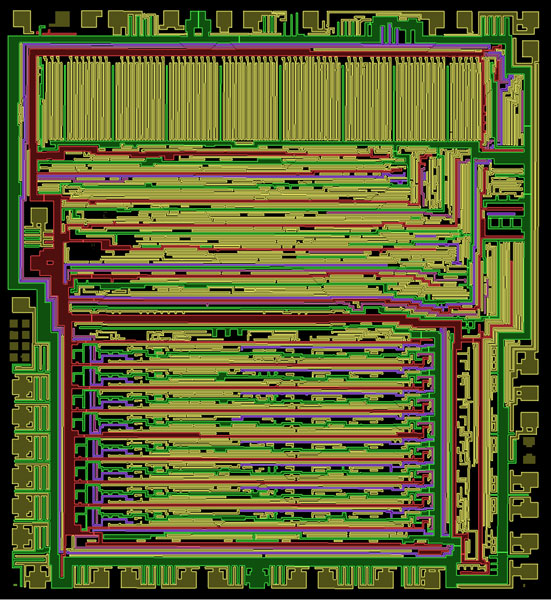
This detailed line drawing of the MOS Technology 6502 microprocessor is a physical description of all the connections between the various circuits on the chip. (Courtesy Greg James, Visual 6502, more in archaeology by Nikhil Swaminathan)

Sep 13, 2011

FAST-SPICE BETA TESTERS WANTED

All participants in the beta-testing program will receive the Symica Fast-SPICE product SymSpice Turbo as a free addition to the Symica tool suite. If you'd like to be a beta tester for the SymSpice Turbo, please send a request to support@symica.com. [more at: http://www.symica.com/news/fast-spice-beta-testers-wanted]

Sep 2, 2011

“The Ugly Duckling,” New Fairy Tales

"The developments of UF process-based “compact” MOSFET models have been reviewed, and exemplary new physical insights on SOI devices attained with the models have been overviewed. Indeed, the UF models have been, and are effective research/education tools. The “ugly duckling” has prevailed, just like in the fairy tale (illustrated in Fig. 10) [19]!" J. G. Fossum

[19] H. C. Anderson, “The Ugly Duckling,” New Fairy Tales. C. A. Reitzel, Copenhagen, Denmark, Nov. 1843.
in
J. Fossum, “UF ‘ Compact ’ Models : A Historical Perspective,” Nanotech, vol. 2, pp. 714 - 719, 2011.

Aug 31, 2011

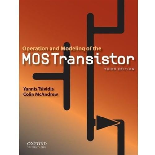
Operation and Modeling of the MOS Transistor

Yannis Tsividis and Colin McAndrew


New to this edition:

  • Energy bands and the energy barrier viewpoint are integrated into the discussion in a smooth, simple manner
  • Expanded discussion of small-dimension effects, including velocity saturation, drain-induced barrier lowering, ballistic operation, polysilicon depletion, quantum effects, gate tunneling current, and gate-induced drain leakage
  • Expanded discussion of small-signal modeling, including gate and substrate current modeling and flicker noise
  • New chapter on substrate nonuniformity and structural effects, discussing transversal and lateral (halo) doping nonuniformity, stress and well proximity effects, and statistical variability
  • A completely re-written chapter on modeling for circuit simulation, covering the considerations and pitfalls in the development of models for computer-aided design
  • Extensively updated bibliography
  • An accompanying website includes additional details not covered in the text, as well as model computer code
ISBN-10: 0195170156 | ISBN-13: 978-0195170153 | Edition: 3

Jul 24, 2011

[mos-ak] Final Program MOS-AK/GSA ESSDERC/ESSCIRC Workshop in Helsinki on Sept.16 2011

Please visit the MOS-AK/GSA Helsinki web site with the final workshop
program:
http://www.mos-ak.org/helsinki/

* Free On-line Registration Form:
http://essderc2011.org/registration_form.php

* Venue: Finlandia Hall in Helsinki, Finland
http://www.essderc2011.org/venue.php

* Agenda: Sept. 16, 2011: 8:30 - 16:30
http://www.mos-ak.org/helsinki/
With panel discussion: "40th Anniversary of SPICE"
(panelists alphabetic list)
Narain D. Arora, Siltera, USA
Christian Enz, EPFL, CH
Chenming Hu, UC Berkeley, USA
Willy Sansen, ESAT-MICAS, B (moderator)
Andrei Vladimirescu, BWRC, UC Berkeley, USA
Andreas Wild, ENIAC - JU, EU

--
You received this message because you are subscribed to the Google Groups "mos-ak" group.
To post to this group, send email to mos-ak@googlegroups.com.
To unsubscribe from this group, send email to mos-ak+unsubscribe@googlegroups.com.
For more options, visit this group at http://groups.google.com/group/mos-ak?hl=en.

Jul 18, 2011

Post Doctoral Researcher / Research Engineer Position in Compact Modeling

The BSIM Group of Electrical Engineering Department at the University of California Berkeley is seeking to hire a bright candidate interested in compact model development/maintenance to join as a post doctoral researcher or research engineer. We are looking for a candidate with PhD (for post doctoral researcher) or Masters (for Research Engineer) degree in EE/Physics preferably for long term (4–5 years). The responsibilities include but not limited to
  • Research and development of new BSIM compact models
  • Maintenance and support of BSIM MOSFET compact models (BSIM4, BSIMSOI and BSIM-MG)
  • Interface with industry to understand requirements and issues with BSIM models and rectify them
  • C & Verilog-A coding and testing/debugging of models
Required skills
  • Excellent semiconductor device physics and process technology knowledge
  • Experience in computer programming (C and Verilog-A)
  • Knowledge of basic analog and digital circuit operation
BSIM Group encourages its members to represent it actively at conferences, workshops, and meetings. Interested applicants should submit their CV to bsimgroup@gmail.com

For more information, please visit:
BSIM Group and Device Group

Jun 29, 2011

Arrays of indefinitely long uniform nanowires and nanotubes

Arrays of indefinitely long uniform nanowires and nanotubes

Nature Materials 10, 494–501 (2011)
doi:10.1038/nmat3038


http://www.nature.com/nmat/journal/v10/n7/full/nmat3038.html


It's frankly nice.... see one of their pictures (hope they don't get too upset!):

Jun 23, 2011

SISPAD 2011 Companion Workshops

September 7, 2011; Hotel Hankyu Expo Park, Osaka, Japan
  • Compact Modeling
    • Organizer: Sadayuki Yoshitomi, Toshiba Corporation
  • Power Devices
    • Organizer: Ichiro Omura, Kyusyu Institute of Technology

SuVolta creates new transistor option for 20 nm

SuVolta creates new transistor option for 20 nm: "SuVolta, a startup process IP company with deep roots indevice design and m..."

Jun 22, 2011

Job offers at RF Micro Devices (RFMD)

I've seen that there are three job offers for Compact Modeling engineers at RFMD:

Tracking Code           Job Title             Location            Date Posted

12134 Senior Modeling Engineer Greensboro, NC, US 6/7/2011
12117 Sr. TCAD Modeling Engineer Greensboro, NC, US 5/26/2011
12116 Sr. Modeling Engineer Greensboro, NC, US 5/24/2011


Note that this is only a re-diffusion of some information we've got, and that we're not related to them in any way!

Jun 17, 2011

Get your own version of Myfab LIMS


Myfab is the Swedish national research infrastructrue for micro and nano fabrication. Use the best cleanroom facilities in Sweden through our laboratory network and bring new scope and opportunity to your research and technical development. [read more]


IMEC benchmarks FinFET superiority

IMEC benchmarks FinFET superiority:

By Peter Clarke, EE Times -- EDN, June 16, 2011

LONDON - The IMEC research institute has compared one planar and two FinFET technologies to see how they perform against scaling and process variability.

The benchmark circuits were six-transistor SRAM cells and SRAM arrays and IMEC has concluded that the FinFET outperforms planar CMOS in variability-aware and technology-aware comparison of SRAM product yield.

Both FinFET on bulk and FinFET on silicon-on-insulaor (SOIFF) technologies come out superior to the planar technology for medium- to large-sized SRAM arrays resulting in higher yields, IMEC said, although it did not disclose the process geometry at which the tests were done. It is likely to have been at around 28 to 22 nm.

As the dimensions of devices scale down, the variations in the electrical parameters of CMOS transistors steadily increase. This is due to random fluctuations in the density of the dopants in the channel, source, and drain. So, two closely placed transistors that are supposedly identical can show a widely different behavior. This makes the design of SRAM memory cells less predictable and controllable for every new technology node.

Because of this scaling 6T planar SRAMs below 22 nm remains challenging, IMEC said. FinFET devices show a lower leakage and variability and it is possible to design more compact cells.

Both FinFET technologies come out as superior to planar for SRAM arrays of greater than 128 kbytes. They are less sensitive to mismatches, thus allowing a more aggressive scaling of the power supply and a lower VCC than planar arrays. For undoped silicon-on-insulator FinFETs (SOIFF), the power supply can be lowered by an additional 200-mV compared to planar. As a sample result: undoped SOIFF FinFET allow for a 95% yield at 0.7-V in 32-Mbit SRAM arrays, moving to Gbit arrays for higher voltages.

Jun 15, 2011

A new birth in the IEEE journals world...

 
Let's welcome them! 
They are starting with some interesting papers on low-power and analog design with nanometer-scale variations.... Let's hope they go on... 
 
IEEE Journal of Emerging and Selected Topics in Circuits and Systems (JETCAS)

We are honored to welcome readers and authors to the inaugural issue of the IEEE Journal on Emerging and Selected Topics in Circuits and Systems (JETCAS for short), which is sponsored by the IEEE Circuits and Systems Society (CAS-S.)

The journal, which is freely accessible on-line to all CAS-S members, aims to build a platform for the broad and timely dissemination of key innovative results and findings in rapidly-growing and/or emerging topic areas within the scope of the IEEE Circuits and Systems Society. Such potentially interdisciplinary emerging topics will be selected as long as, first, they are clearly situated at the forefront of current scientific and technological developments and, second, they are expected to grow over time in scientific and professional importance and, therefore, in the number of active practitioners. From this point of view, JETCAS is expected to create new communities interested in the long-term development of the most promising subjects presented in the journal. The editorial strategy followed by JETCAS will be the publication of Special Issues on the selected topics. These issues will include research contributions from leading experts and presentations geared towards a wide audience of scientists and pra

MASSOUD PEDRAM, Editor-in-Chief (EiC)

MANUEL DELGADO-RESTITUTO, Deputy EiC

ENRICO MACII, 2010-2011 VP Publications, IEEE CAS-S

GIANLUCA SETTI, 2010 President, IEEE CAS-S  


Volume 1, Issue 1 - Inaugural Edition
http://ieeexplore.ieee.org/xpl/RecentIssue.jsp?punumber=5503868

Pedram, M.;  Delgado-Restituto, M.;  Macii, E.;  Setti, G., Inaugural Editorial
http://ieeexplore.ieee.org/stamp/stamp.jsp?tp=&arnumber=5765455

-----------------------------------------------------------------------------------------------------
Variation-Aware Design for Nanoscale VLSI Circuits and Systems
The focus of this issue is on the challenges faced in designing digital and analog circuits in nanoscale technologies, where variations due to process, environmental, and aging variations are substantial.  The root causes of these effects can generally be traced to scaling: with the drive towards even greater miniaturization, these problems become even more acute and it is imperative that they be addressed.  The solutions involve the invention of improved design techniques, better design automation, and closer interactions between the phenomenological root causes and the designer.  The six papers in this issue attempt to provide a view of the landscape, reflecting the current state of the art and future directions.

Sapatnekar, S. S., Guest Editorial
http://ieeexplore.ieee.org/stamp/stamp.jsp?tp=&arnumber=5762378

------------------------------------------------------------------------------------------------------------------
Sapatnekar, S. S., Overcoming Variations in Nanometer-Scale Technologies
http://ieeexplore.ieee.org/stamp/stamp.jsp?tp=&arnumber=5762377
Nanometer-scale circuits are fundamentally different from those built in their predecessor technologies in that they are subject to a wide range of new effects that induce on-chip variations. These include effects associated with printing finer geometry features, increased atomic-scale effects, and increased on-chip power densities, and are manifested as variations in process and environmental parameters and as circuit aging effects. The impact of such variations on key circuit performance metrics is quite significant, resulting in parametric variations in the timing and power, and potentially catastrophic failure due to reliability and aging effects. Such problems have led to a revolution in the way that chips are designed in the presence of such uncertainties, both in terms of performance analysis and optimization. This paper presents an overview of the root causes of these variations and approaches for overcoming their effects.
-----------------------------------------------------------------------------------------------------------------
Karakonstantis, G.;  Chatterjee, A.;  Roy, K., Containing the Nanometer "Pandora-Box": Cross-Layer Design Techniques for Variation Aware Low Power Systems
http://ieeexplore.ieee.org/stamp/stamp.jsp?tp=&arnumber=5766061
The demand for richer multimedia services, multifunctional portable devices and high data rates can only been visioned due to the improvement in semiconductor technology. Unfortunately, sub-90 nm process nodes uncover the nanometer Pandora-box exposing the barriers of technology scaling-parameter variations, that threaten the correct operation of circuits, and increased energy consumption, that limits the operational lifetime of today's systems. The contradictory design requirements for low-power and system robustness, is one of the most challenging design problems of today. The design efforts are further complicated due to the heterogeneous types of designs (logic, memory, mixed-signal) that are included in today's complex systems and are characterized by different design requirements. This paper presents an overview of techniques at various levels of design abstraction that lead to low power and variation aware logic, memory and mixed-signal circuits and can potentially assist in meeting the strict power b
-----------------------------------------------------------------------------------------------------------------
Mitra, S.;  Brelsford, K.;  Kim, Y. M.;  Lee, H.-H. K.;  Li, Y., Robust System Design to Overcome CMOS Reliability Challenges
http://ieeexplore.ieee.org/stamp/stamp.jsp?tp=&arnumber=5751208
Today's mainstream electronic systems typically assume that transistors and interconnects operate correctly over their useful lifetime. With enormous complexity and significantly increased vulnerability to failures compared to the past, future system designs cannot rely on such assumptions. For coming generations of silicon technologies, several causes of hardware reliability failures, largely benign in the past, are becoming significant at the system level. Robust system design is essential to ensure that future systems perform correctly despite rising complexity and increasing disturbances. This paper describes three techniques that can enable a sea change in robust system design through cost-effective tolerance and prediction of failures in hardware during system operation: 1) efficient soft error resilience; 2) circuit failure prediction; and 3) effective on-line self-test and diagnostics. The need for global optimization across multiple abstraction layers is also demonstrated.
-----------------------------------------------------------------------------------------------------------------
Seok, M.;  Chen, G.;  Hanson, S.;  Wieckowski, M.;  Blaauw, D.;  Sylvester, D., CAS-FEST 2010: Mitigating Variability in Near-Threshold Computing
http://ieeexplore.ieee.org/stamp/stamp.jsp?tp=&arnumber=5762379
Near threshold computing has recently gained significant interest due to its potential to address the prohibitive increase of power consumption in a wide spectrum of modern VLSI circuits. This tutorial paper starts by reviewing the benefits and challenges of near threshold computing. We focus on the challenge of variability and discuss circuit and architecture solutions tailored to three different circuit fabrics: logic, memory, and clock distribution. Soft-edge clocking, body-biasing, mismatch-tolerant memories, asynchronous operation and low-skew clock networks are presented to mitigate variability in the near threshold ${V} _{rm DD}$ regime.
-----------------------------------------------------------------------------------------------------------------
Maricau, E.;  Gielen, G., Computer-Aided Analog Circuit Design for Reliability in Nanometer CMOS
http://ieeexplore.ieee.org/stamp/stamp.jsp?tp=&arnumber=5762376
Integrated analog circuit design in nanometer CMOS technologies brings forth new and significant reliability challenges. Ever-increasing process variability effects and transistor wear-out phenomena such as BTI, hot carrier degradation and dielectric breakdown force designers to use large design margins and to increase the uncertainty on the circuit lifetime. To help designers to tackle these problems at design time (i.e., Design For Reliability, or DFR), accurate transistor aging models, efficient circuit reliability analysis methods and novel design techniques are needed. The paper overviews the current state of the art in DFR for analog circuits. The most important unreliability effects in nanometer CMOS technologies are reviewed and transistor aging models, intended for accurate circuit simulation, are described. Also, efficient methods for circuit reliability simulation and analysis are discussed. These methods can help designers to analyze their circuits and to identify weak spots. Finally, cost-effect
-----------------------------------------------------------------------------------------------------------------
Zhang, X.;  Mukadam, M. Y.;  Mukhopadhyay, I.;  Apsel, A. B., Process Compensation Loops for High Speed Ring Oscillators in Sub-Micron CMOS
http://ieeexplore.ieee.org/stamp/stamp.jsp?tp=&arnumber=5756255
In this paper, we present two implementations of a closed-loop process compensation scheme for high speed ring oscillators-the comparator based and the switched capacitor based loops. We provide detailed discussion of the frequency accuracy, loop stability, and implementation cost for each design. More than 150 test chips from multiple wafer-runs in a 90 nm CMOS process verify that frequency accuracy of better than 2.6% can be achieved with the application of the proposed compensation loop. Moreover, by leveraging a low variation addition-based current source, we have demonstrated a fully-integrated 2.15 GHz ring oscillator with less than 4.6% frequency variation without external references or post fabrication calibration, which is 3.8 $times$ improvement in frequency accuracy over the baseline case. The same compensation scheme can also alleviate frequency drift caused by temperature.

JETCAS is published quarterly and solicits, with particular emphasis on emerging areas, special issues on topics that cover the entire scope of the IEEE Circuits and Systems (CAS) Society, namely the theory, analysis, modeling, design, automation, and implementation of electronic circuits and systems, spanning theoretical foundations, applications, and architectures for signal and information processing.

Jun 13, 2011

First Graphene Integrated Circuit


IBM researchers have built the first IC based on a graphene transistor. It is another step toward overcoming the limits of silicon and a potential path to flexible electronics [read more at spectrum.ieee.org]

Jun 10, 2011

Alternative semiconductor fabrication methods enable inexpensive, conformable consumer devices - Solid State Technology

Alternative semiconductor fabrication methods enable inexpensive, conformable consumer devices - Solid State Technology

Emerging technology and a developing infrastructure for printed electronics is enabling circuitry that is flexible, conformable, and inexpensive to mass-produce. FlexTech Alliance has identified, funded, and directed advanced development in the flexible and printed electronics infrastructure, paving the way for the practical manufacture of a variety of low-cost applications such as electronic packaging, ID tags, and wide-area lighting panels.

Printed electronics include a set of consumer markets where printed logic and memory will be required. The size and cost of fully printed systems is set to challenge silicon-based technologies in ultra-high-volume distributed applications. To address this issue, Norwegian firm ThinFilm Electronics produces rewritable memory tags manufactured using full roll-to-roll (R2R) printing. Printed non-volatile RAM (NVRAM), when combined with printed transistor elements, serves as the basis of a new generation of cheap, disposable, and highly ubiquitous electronic devices. The company is working with major toy and game companies and has established high-volume manufacturing to deliver millions of tags per month.

In other commercial development, a new method for fabricating printed semiconductors, developed by NthDegree Technologies, allows a standard high-speed printing press to print conductive ink on to paper, plastic, or other substrate materials. Printed semiconductors made with these inks reduce the cost of producing semiconductor-based devices while creating innovative conformable products. Wide-area lighting is currently being produced with this technology by means of a light-emitting diode (LED) "ink". This LED ink is being used to print area lighting that is converted into a flat panel to replace fluorescent tube fixtures.

These latest developments in printed electronics materials, tools and processes, including LED lighting and printed memory, will be discussed and demonstrated at the Extreme Electronics TechXpot session "Printed electronics: Beyond R&D to real-deal technologies," presented by the FlexTech Alliance at SEMICON West, July 14, 2011. For more information about FlexTech Alliance visit www.flextech.org.

Freescale's Su calls for improved EDA tools

Freescale's Su calls for improved EDA tools:

As more embedded devices are being connected to the "Internet of things" the design methodologies used in IC designs need to change accordingly for faster chip turnarounds.

Lisa Su, VP and general manager of FreescaleLisa Su, VP and general manager of Freescale"Some 7 billion devices will be connected to the Internet in this era from 2006 to 2020," said Lisa Su, vice president and general manager of Freescale Semiconductor Inc's networking and multimedia group. "And mobile traffic is doubling every year through 2015."

Su delivered the Tuesday (June 7) keynote here at the Design Automation Conference, whose organizers have placed embedded systems and software squarely in the apex of DAC with dedicated exhibit areas on the show floor.

While only 15 exhibitors specifically identified themselves as embedded hardware/software providers out of a total of 200, the technical program was loaded with embedded presentations and Su's keynote was clearly aimed at showing that at least Freescale understands that it is operating in a new space for them, the embedded world.

"The embedded era is defined by standards-based hardware and software, is open source, and aimed numerous markets, including health, safety, energy, transportation, communications, entertainment, automation, and, of course, cloud computing," said Su.

Su quoted statistics that the monthly mobile traffic will increase tenfold from today's 0.6 exabytes to 6.3 exabytes by 2015. "The resultant heterogeneous networks, together with the increasing needs of the ‘connected' car, offer many opportunities to semiconductor companies like us," said Su.

The many-core paradigm of the expected SOC technology transition poses a few challenges, according to Su.

Among these are scalability as the number of cores per processor generation will double. Also there will be system tradeoffs to consider between cores versus using hardware acceleration, as well cluster optimization among cores, caches, local vs. global resource sharing. And an increasing amount of high-speed mixed-signal I/O will place strain on expected quality of service metrics.

read more...

Jun 8, 2011

Postdoc Position in Thin Films (Thun, CH)

Empa is the interdisciplinary research and services institution for material sciences and technology development of the ETH Domain. Laboratory for Mechanics of Materials and Nanostructures at Empa's location in Thun, CH, is offering an Academia / Industry Postdoc Position in Thin Films

Submit your application online and upload all documents through this webpage by June 30, 2011:
http://internet1.refline.ch/673276/0190/++publications++/1/index.html

Additional information can be obtained from the EMPA website and by contacting Dr. Johann Michler.

IEDM'2011 Abstract Submission Site is Now Open (Deadline: June 24, 2011)

IEDM Abstract Submission Site is Now Open - Abstract Submission
Deadline:   June 24, 2011

2011 IEEE International Electron Devices Meeting
The Annual Technical Meeting of the Electron Devices Society will be held at the
Washington Hilton, Washington, DC USA  - December 5-7, 2011

To view the IEDM Call for Papers and instructions for submitting an abstract to
the conference, visit:      http://www.ieee-iedm.org

IEEE International Electron Devices Meeting (IEDM) is the world’s pre-eminent
forum for reporting technological breakthroughs in the areas of semiconductor
and electronic device technology, design, manufacturing, physics, and modeling. 
IEDM is the flagship conference for nanometer-scale CMOS transistor technology,
advanced memory, displays, sensors, MEMS devices, novel quantum and nano-scale
devices and phenomenology, optoelectronics, devices for power and energy
harvesting, high-speed devices, as well as process technology and device
modeling and simulation.  

Starting this year (2011) there is an increased emphasis on circuit and device
interaction.  With ever increasing transistor count, nanometer design rules and
layout restrictions, circuit-device interaction is becoming critical to
providing viable technology solutions. This new emphasis includes
technology/circuit co-optimization, power/performance/area analyses, design for
manufacturing and process control, as well as CMOS platform technology and
scaling.

INCREASED PARTICIPATION IN THE FOLLOWING AREAS IS SOUGHT: 
 * Circuit-device interaction 
 * Energy harvesting
 * Biomedical devices
 * Power devices

Information about IEDM can be found at: http://www.ieee-iedm.org 
Twitter: http://twitter.com/ieee_iedm 
Facebook: http://www.facebook.com/pages/IEDM/131119756449 

MEETING HIGHLIGHTS 
 * New subcommittees (Circuit-Device Interaction and Nano Device Technology)
 * New for 2011:  90 Minute Tutorial Sessions on Emerging Topics, Saturday
afternoon, December 3
 * Three plenary presentations by prominent experts 
 * Invited papers on all aspects of advanced devices and technologies.
 * An Emerging Technology session. 
 * Two evening Panel discussions.
 * Presentation of IEEE/EDS awards. 
 * IEDM Luncheon presentation will be held on Tuesday, December 6.
 * Two short courses will be held on Sunday, December 4.

Further Information - All questions or inquiries for further information
regarding this meeting should be directed to the Conference Office at:

19803 Laurel Valley Place
Montgomery Village, MD 20886 USA
Tel: 301-527-0900, ext. 2
Email: iedm@his.com 
Local European Contact 

Stefan De Gendt, IMEC, Belgium
Local Asian Contact 
Norikatsu Takaura, LEAP, Japan
2011 Conference Chair 
Kazunari Ishimaru, Toshiba, Japan
Technical Program Chair 
Veena Misra, North Carolina State University, USA

If you know of any colleagues who may have a paper to contribute and have not
received this notice, please bring it to their attention.

Jun 3, 2011

Course on Statistical CMOS Variability and Reliability, San Jose CA, June 13th and 14th

Professor Asen Asenov, CEO of Gold Standard Simulations, will be delivering a comprehensive course (see the flyer) on variability and reliability issues and their impact on modern CMOS devices and design.

The course topics include, Variability classification,Sources of statistical variability, Simulation of statistical variability, Variability trends in conventional and novel MOSFETs, Random telegraph noise statistics, Statistical aspects of reliability, Statistical compact model strategies and Statistical circuit simulation. At this event there will also be a special lecture on Variability in FinFET devices.

For more information please visit: http://www.goldstandardsimulations.com/courses/ or get in touch with them at courses(at)goldstandardsimulations.com.