Feb 23, 2021

[papers] Compact/SPICE Modeling

[1] Wang, Jie; Chen, Zhanfei; You, Shuzhen; Bakeroot, Benoit; Liu, Jun; Decoutere, Stefaan; "Surface-Potential-Based Compact Modeling of p-GaN Gate HEMTs" Micromachines (2021) 12, no. 2: 199; https://doi.org/10.3390/mi12020199

Abstract: We propose a surface potential (SP)-based compact model of p-GaN gate high electron mobility transistors (HEMTs) which solves the Poisson equation. The model includes all possible charges in the GaN channel layer, including the unintended Mg doping density caused by out-diffusion. The SP equation and its analytical approximate solution provide a high degree of accuracy for the SP calculation, from which the closed-form I–V equations are derived. The proposed model uses physical parameters only and is implemented in Verilog-A code.

Fig: The equivalent circuit of the capacitance of field plates (FPs) of a p-GaN gate HEMT.


[2] Chen, H. and He, L.,  The spatial and energy distribution of oxide trap responsible for 1/f noise in 4H-SiC MOSFETs. Journal of Physics Communications, JPCO-101816.R1 (2021)

Abstract: Low-frequency noise is one of the important characteristics of 4H-SiC metal-oxide-semiconductor field-effect transistors (MOSFETs) that is susceptible to oxide traps. Drain-source voltage noise models of 4H-SiC MOSFETs under low–drain-voltage and inverse condition were proposed by considering the spatial and energy non-uniform distribution of the oxide trap, based on the McWhoter model for uniform trap distribution. This study performed noise experiments on commercial 4H-SiC MOSFETs, and revealed that the non-uniform spatial and non-uniform energy distribution caused new 1/f noise phenomenon, different from that under uniform spatial and energy distribution. By combining experimental data and theoretical models, the spatial and energy distribution of oxide traps of these samples were determined.
Fig: Adaptive circuit for 4H-SiC MOSFET noise measurement
in the frequency 1 Hz-10kHz ranged


Feb 22, 2021

[Kioxia] Less is more: the challenge of #3D-#NAND memory https://t.co/N5eEZAOL16 #semi https://t.co/Tm7fNXTynD


from Twitter https://twitter.com/wladek60

February 22, 2021 at 06:24PM
via IFTTT

#TSMC vs #Intel https://t.co/kNtoOcTRFx #semi @mannerisms @semiwiki https://t.co/eMLyKrFdY1


from Twitter https://twitter.com/wladek60

February 22, 2021 at 02:49PM
via IFTTT

[https://t.co/FrgrQhA6mP] #India needs chipset manufacturers — lots of them. Here is why. https://t.co/VrJw27rpFp #semi https://t.co/nq0KKtrJVP


from Twitter https://twitter.com/wladek60

February 22, 2021 at 02:07PM
via IFTTT

[3D Printing Industry] Researchers open up low-cost #opensource #microfluidics #3D printing - https://t.co/VwPoWIzI72 #semi https://t.co/OyfmccoCb9


from Twitter https://twitter.com/wladek60

February 22, 2021 at 02:04PM
via IFTTT

Feb 19, 2021

Virtual Si Museum /2107/ TG4 and TG50

The TG1-TG5 series transistor are the first industrially mass-produced BJT transistors in Poland. The serial production was started by the TEWA Semiconductor Factory, Warsaw, in early1960s. Then, the TG50-TG55 series, was also manufactured by the TEWA in 1961–1962. 

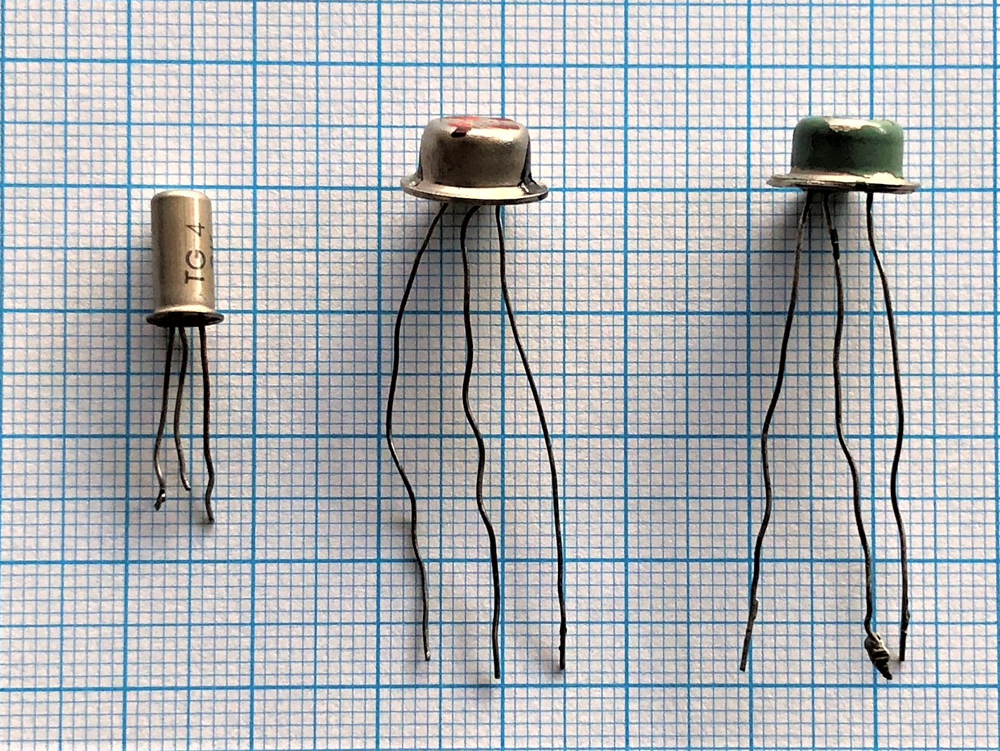
The TG4 (see Pic: below) is low power, low frequency, pnp germanium (Ge) alloy transistor (with 75 mW max collector power) [1].

The TG50 (below) is medium power, low frequency,  pnp germanium (Ge) alloy transistor (with 175 mW max collector power) [2].

An initial stage of Polish semiconductor microelectronics research activities has been reviewed by Prof. Jerzy Pułtorak. In his paper [3], he has reviewed activities of leading Polish R&D groups starting from Department of Electronics, Polish Academy of Sciences (PAN) founded on July 4, 1952 till foundation of the Instytut Technologii Elektronowej (ITE, Warsaw) early 1960 (now Sieć Badawcza Łukasiewicz - Instytut Mikroelektroniki i Fotoniki).  The first, in Poland, experimental germanium point-contact transistor TP-1 [4] has been developed by Prof. Rosinski just after John Bardeen, Walter Brattain and William Shockley have invented a semi-conductor triode (transistor) [5] on December 23, 1947.

Pic: TG4 and two TG50 by the TEWA Semiconductor Factory, Warsaw (PL)

References: 
[1] TG1-5 / PL Wikipedia/ https://pl.wikipedia.org/wiki/TG1-5
[2] TG50-5  / PL Wikipedia/ https://pl.wikipedia.org/wiki/TG50-55
[3] J. Pułtorak, "60 years of polish transistors," 2014 Proceedings of the 21st International Conference Mixed Design of Integrated Circuits and Systems (MIXDES), Lublin, Poland, 2014, pp. 15-21, doi: 10.1109/MIXDES.2014.6872144.
[4] W.Rosinski, J.Groszkowski, “Doswiadczalne tranzystory punktowe model TP” (“Experimental point-cotact transistors model TP”), Arch. Elektrot. 4, 1955, p. 381
[5] J.Bardeen, H.W.Brattain, “The transistor, a semi-conductor triode”, Phys.Rev.74, 7, 1954, p.230