May 4, 2020

[paper] Benchmark Tests for MOSFET Thermal Noise Models

Scholten A.J., Smit G.D.J., Pijper R.M.T., Tiemeijer L.F.
Benchmark Tests for MOSFET Thermal Noise Models
In: Grasser T. (eds) Noise in Nanoscale Semiconductor Devices. Springer, Cham

Abstract - In today’s semiconductor industry, many traditional integrated device manufacturers (IDMs) are moving away from chip manufacturing, and transforming into fabless companies that use foundry services for manufacturing their ICs. This is especially true in the field of advanced CMOS technologies. In these companies-under-transformation, the work of the modeling engineer is changing: instead of building models from scratch themselves, most companies choose to use the modeling packages that are delivered by the foundries. There are two reasons to be skeptical about RF noise models. First, measurement of noise, and RF noise in particular, is a difficult and specialist topic. One should not take for granted that every company has the required expertise to carry out this task successfully. A second reason to check RF noise models is that the most popular compact MOSFET models are BSIM4 [1] and BSIMBULK [2], which are not particularly strong and certainly not predictive when it comes to RF noise. As a consequence, the work of the modeling engineer is changing from model creation to model verification.

Tab: Overview of benchmark tests for thermal noise
#No
Bias
Length
Quantity
Test
Remark
#1
VDS = 0V
All
SID
γ = 1

#2
VDS = 0 V
All
SIG
β = 5/12

#3
VDS = 0 V
All
c
c = 0
In the limit f ↓ 0 Hz
#4
Weak Inv
All
SID
F = 1
Disregard SIG contributions from gate to drain
#5
Saturation
Long
SID
γ = 2/3

#6
Saturation
Long
SIG
β = 4/3

#7
Saturation
Long
c
c = 0.4j

#8
Saturation
Short
SID
γ enhancement
Switch off gate resistance
#9
Saturation
All
SID
γ D,NMOS ≥ γ D,PMOS
Switch off gate resistance
#10
Saturation
All
SID
Different Vth flavors should nearly coincide
When plotted against ID


First Online: 27 April 2020
DOI: 10.1007/978-3-030-37500-3_20

Ref: 
[1] N. Paydavosi, T.H. Morshed, D.D. Lu, W. Yang, M.V. Dunga, X. Xi, J. He, W. Liu, K.M. Cao, X. Jin, J.J. Ou, M. Chan, A.M. Niknejad, C. Hu, BSIM4v4.8.0 MOSFET Model - User’s Manual. [Online]. Available: http://bsim.berkeley.edu/models/bsim4/
[2] H. Agarwal, C. Gupta, H.-L. Chang, S. Khandelwal, J.P. Duarte, Y.S. Chauhan, S. Salahuddin, C. Hu, BSIM-BULK106.2.0 MOSFET Compact Model - Technical Manual. [Online]. Available: http://bsim.berkeley.edu/models/bsimbulk/

[paper] DHBT with Record ft of 813 GHz

Y. Shiratori, T. Hoshi and H. Matsuzaki,
InGaP/GaAsSb/InGaAsSb/InP Double Heterojunction Bipolar Transistors
With Record ft of 813 GHz
IEEE EDL vol. 41, no. 5, pp. 697-700, May 2020
doi: 10.1109/LED.2020.2982497

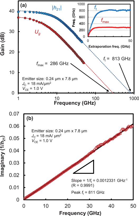
Abstract - We fabricated InGaP/GaAsSb/InGaAsSb/InP double heterojunction bipolar transistors (DHBTs) with an aggressive lateral and vertical scaling technology to improve the current gain cutoff frequency (fT) further. A 13-nm-thick GaAsSb/InGaAsSb base and a 40-nm-thick InP collector are used to reduce electron transit time. In addition, the width of the base electrode on each side of the emitter is reduced to about 0.05µm to suppress increases in parasitic collector capacitance. A fabricated DHBT with the emitter size of 0.24µm×7.8 µm exhibits maximum differential current gain of ∼95 and collector-emitter breakdown voltage of 2.6V. At a collector current density of 18 mA/µm2, the DHBT exhibits fT of 813 GHz, which is the highest among all types of transistors measured at a room temperature.
Fig: (a) Current gain ( |h21| ) and Mason’s unilateral power gain (Ug ) of the DHBT as a function of frequency. JC and VCE are 18 mA/μm2 and 1.0 V, respectively. ft and fmax are extrapolated by single-pole fitting. Inset: frequency dependence of extrapolating ft and fmax . (b) Gummel’s ft extraction (imaginary part of 1/h21 as a function of frequency). The red circles and black line show experimental data and a linear fitting, respectively.

URL: https://ieeexplore.ieee.org/stamp/stamp.jsp?tp=&arnumber=9044299&isnumber=9079222

May 1, 2020

[paper] Physical Mechanisms of Reverse DIBL and NDR in FeFETs With Steep Subthreshold Swing

C. Jin, T. Saraya, T. Hiramoto and M. Kobayashi,
in IEEE J-EDS, vol. 8, pp. 429-434, 2020
doi: 10.1109/JEDS.2020.2986345

Abstract - We have investigated transient IdVg and IdVd characteristics of ferroelectric field-effect transistor (FeFET) by simulation with ferroelectric model considering polarization switching dynamics. We show transient negative capacitance (TNC) with polarization reversal and depolarization effect can result in sub-60mV/dec subthreshold swing (SS), reverse drain-induced barrier lowering (R-DIBL), and negative differential resistance (NDR) without traversing the quasi-static negative capacitance (QSNC) region of the S-shaped polarization-voltage (PV) predicted by single-domain Landau theory. Moreover, the mechanisms of R-DIBL and NDR based on the TNC theory are discussed in detail. The results demonstrated in this work can be a possible explanation for the mechanism of previously reported negative capacitance field-effect transistor (NCFET) with sub-60mV/dec SS, R-DIBL, and NDR.
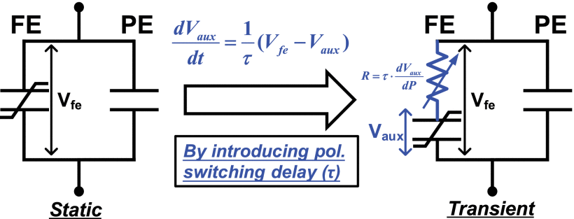
Equivalent circuits of a ferroelectric capacitor in both static and transient conditions.

Apr 30, 2020

#paper: W. E. Muhea, G. U. Castillo, H. C. Ordoñez, T. Gneiting, G. Ghibaudo and B. Iñiguez, "Parameter Extraction and Compact Modeling of 1/f Noise for Amorphous ESL IGZO TFTs," in IEEE J-EDS, vol. 8, pp. 407-412, 2020. https://t.co/SCTs7BsGJZ https://t.co/gZcCgMrYVd


from Twitter https://twitter.com/wladek60

April 30, 2020 at 03:13PM
via IFTTT

#paper: J. Leise et al., "Charge-Based Compact Modeling of Capacitances in Staggered Multi-Finger OTFTs," in IEEE J-EDS, vol. 8, pp. 396-406, 2020. https://t.co/zk4BAp2tMj https://t.co/Ay502xHy1w

#paper: J. Leise et al., "Charge-Based Compact Modeling of Capacitances in Staggered Multi-Finger OTFTs," in IEEE J-EDS, vol. 8, pp. 396-406, 2020


https://t.co/zk4BAp2tMj pic.twitter.com/Ay502xHy1w

— Wladek Grabinski (@wladek60) April 30, 2020 from Twitter https://twitter.com/wladek60

#Spanish and #French governments turn to Jitsi Meet #opensource video-conferencing platform https://t.co/68ZzP2iPq2 https://t.co/uXUBtMOAli


from Twitter https://twitter.com/wladek60

April 30, 2020 at 10:05AM
via IFTTT

Apr 29, 2020

#paper: K. Xia, "New C∞ Functions for Drain–Source Voltage Clamping in Transistor Modeling," in IEEE TED, vol. 67, no. 4, pp. 1764-1768, April 2020. https://t.co/N9yGopiPNg https://t.co/9AKubeYY5x


from Twitter https://twitter.com/wladek60

April 29, 2020 at 04:16PM
via IFTTT