Y. Shiratori, T. Hoshi and H. Matsuzaki,
InGaP/GaAsSb/InGaAsSb/InP Double Heterojunction Bipolar Transistors
With Record ft of 813 GHz
IEEE EDL vol. 41, no. 5, pp. 697-700, May 2020
doi: 10.1109/LED.2020.2982497
Abstract - We fabricated InGaP/GaAsSb/InGaAsSb/InP
double heterojunction bipolar transistors (DHBTs) with
an aggressive lateral and vertical scaling technology to
improve the current gain cutoff frequency (fT) further.
A 13-nm-thick GaAsSb/InGaAsSb base and a 40-nm-thick
InP collector are used to reduce electron transit time.
In addition, the width of the base electrode on each side
of the emitter is reduced to about 0.05µm to suppress
increases in parasitic collector capacitance. A fabricated
DHBT with the emitter size of 0.24µm×7.8 µm exhibits maximum differential current gain of ∼95 and collector-emitter
breakdown voltage of 2.6V. At a collector current density
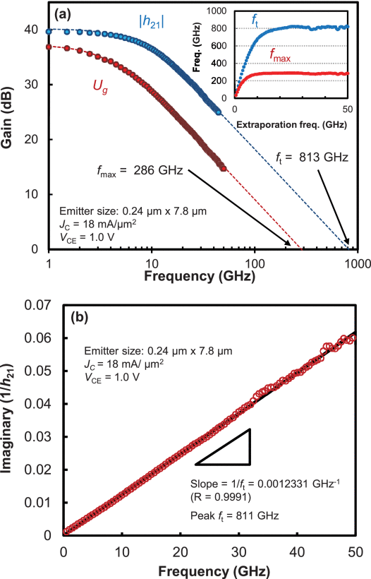
of 18 mA/µm2, the DHBT exhibits fT of 813 GHz, which is the
highest among all types of transistors measured at a room
temperature.
 |
Fig: (a) Current gain ( |h21| ) and Mason’s unilateral power gain (Ug ) of the DHBT as a function of frequency. JC and VCE are 18 mA/μm2 and 1.0 V, respectively. ft and fmax are extrapolated by single-pole fitting. Inset: frequency dependence of extrapolating ft and fmax . (b) Gummel’s ft extraction (imaginary part of 1/h21 as a function of frequency). The red circles and black line show experimental data and a linear fitting, respectively.
URL: https://ieeexplore.ieee.org/stamp/stamp.jsp?tp=&arnumber=9044299&isnumber=9079222
