Jan 24, 2024

[C4P] RISC-V Summit Europe


The RISC-V Summit Europe is the premier event that connects the European movers and shakers - from industry, government, research, academia and ecosystem support - that are building the future of innovation on RISC-V.
RISC-V, the open standard instruction set architecture (ISA), is enabling a range of new applications and research that will define the future of computing in Europe. The region has been central to RISC-V’s success, with one-third of RISC-V’s global community based in Europe. 
RISC-V Summit Europe takes place from Monday 24th to Friday 28th June, 2024. The combination of strong industrial and academic communities is key to the success of RISC-V in Europe, and for this reason the conference is designed to help attendees to explore both commercial and research applications.

Present your work
Presentations on inspirational ideas and technical progress are invited to present 
at RISC-V Summit Europe.

RISC-V Summit Europe brings together developers, architects, technical decision and policy makers from across the European RISC-V ecosystem. Attendees from academia, research, SMEs, industry, and open source communities will come together to exchange knowledge, ideas, technologies, and research, shaping the future of RISC-V computing in Europe.

Taking place from June 24-28, 2024, the event will have a single track of keynotes, invited and selected talks, alongside an exhibition showcasing the latest developments across industry and research, including technology demonstrations and poster sessions. Submissions are invited either for:
🚀  Industry Sessions
Exciting large-scale research efforts, announcement and success-stories.
👩‍🔬  R&D Sessions

Leading edge academic and industry research & development insights.


Important dates
  • Abstract submission deadline: March 15th, 2024, AoE (Anywhere on Earth).
  • Author notification: April 29th, 2024.
  • Final abstract PDF and slides deadline: May 31st, 2024 AoE.
  • Poster PDF deadline: June 14, 2024 AoE.
  • RISC-V Summit Europe: June 24-28, 2024, Munich.
The Steering Committee aims to provide a limited budget for stipends. More information will be available on the conference website before the submission deadline.


Jan 23, 2024

[C4P] OSDA 2024

4th Workshop on Open-Source Design Automation
March 25, 2024, 14:00-18:00
and will be co-hosted with DATE Conference
in VCC in Valencia, Spain

There is no doubt that proprietary EDA tools are successful, mature, and fundamental for hardware development. However, the “walled garden” approach created by closed-source tool flows can hamper novel FPGA/ASIC-based applications and EDA innovation alike by requiring that researchers either operate within the limits of what has already been imagined, or require that they attempt to simulate their effects on incomplete models, potentially leading to incorrect conclusions.

Another recent development has been growing activity in the open-source community to produce open equivalents of EDA tools, as well as efforts to document FPGA architectures. For instance, Yosys has been widely used for behavioral synthesis since 2012 and Project Icestorm, the first fully open-source FPGA design flow has been available since 2015; together they enabled Trenz Electronic’s icoBOARD, a Raspberry Pi accessory that could be programmed entirely using its ARM CPU, a platform not otherwise supported by the vendor. The availability of low-cost FPGA development boards such as the icoBOARD, TinyFPGA, IceZUM Alhambra, the iceBreaker board, amongst others have also played a part in fostering this “Open FPGA” movement. With OpenLANE and the Skywater process development kit, an open-source tool flow emerged that synthesizes RTL models to GDSII, gracefully enabling open-source ASIC design. The advantages of open design automation -- as Linux has provided for operating systems -- are many: unrestricted research and development, improved quality due to competition, teaching benefits, as well as lowering the barrier and risk to entry, and time to market, of start-ups for building novel applications, tools, and silicon. With such an open-source ecosystem in place, ASICs and reprogrammable logic could achieve the same success and inspire the next generation of hardware engineers as the Raspberry Pi has done for software engineers.

OSDA intends to provide an avenue for industry, academics, and hobbyists to collaborate, network, and share their latest visions and open-source contributions, with a view to promoting reproducibility and re-usability in the design automation space. DATE provides the ideal venue to reach this audience since it is the flagship European conference in this field -- particularly poignant due to the recent efforts across the European Union (and beyond) that mandate “open access” for publicly funded research to both published manuscripts as well as software code necessary for reproducing its conclusions. A secondary objective of this workshop is to provide a peer-reviewed forum for researchers to publish “enabling” technology such as infrastructure or tooling as open-source contributions -- standalone technology that would not normally be regarded as novel by traditional conferences -- such that others inside and outside of academia may build upon it.

Topics - we request contributions of the following topics, including but not limited to:
  • Open-source EDA tools -- the latest developments, breakthroughs, challenges and surveys on the toolflows required to target real silicon parts: synthesis, verification, place and route, etc.
  • Open-source IP -- contributions that enrich the IP ecosystem and reduce the need to “re-invent the wheel”, e.g. PCIe and DDR controllers, debug infrastructure, etc.
  • Design methodologies provided as open-source -- such as hardware description languages (e.g. MyHDL, Chisel), domain specific (DSL), high level synthesis (HLS), or asynchronous methods.
  • Directions on where the open-source EDA movement should go, current weaknesses in the toolchain, and/or perspectives from industry on how open-source can affect aspects of safety, security, verification, IP protection, time-to-market, datacenter/cloud infrastructure, etc.
  • Discussions and case studies on how to license, acquire funding, and commercialize technologies surrounding open-source hardware, which may be different to open software.
Important Dates
Event Date
Early-Bird submission Jan. 20, 2024
Early-Bird notification Jan 23, 2024
Regular submission deadline Feb. 15, 2024
Regular notification Feb. 22, 2024
Camera-ready final version March 16, 2024
Workshop March 25, 2024, 14:00-18:00

Organizing committee
  • Christian Krieg (OSDA and TU Wien, Austria)
  • Matthew Guthaus (UC Santa Cruz, USA)
  • Claire Xenia Wolf (YosysHQ, Austria)
Program committee
  • Andrea Borga
  • Jean-Paul Chaput
  • Tim Edwards
  • Xin Fang
  • Francesco Gonnella
  • Daniel Grosse
  • Matthew Guthaus
  • Hipolito Guzman-Miranda
  • Steve Hoover
  • Tsung-Wei Huang
  • Andrew Kahng
  • Lucas Klemmer
  • Dirk Koch
  • Christian Krieg
  • Jim Lewis
  • Mieszko Lis
  • Steffen Reith
  • Stefan Riesenberger
  • Davide Rossi
  • Frans Skarman
  • Antonino  Tumeo
  • Vamsi Vytla

Jan 18, 2024

[paper] Open-source design of integrated circuits

Patrick Fath, Manuel Moser, Georg Zachl. Harald Pret
Open-source design of integrated circuits
Elektrotech. Inftech. (2024)
DOI: 10.1007/s00502-023-01195-5

* Institute for Integrated Circuits, Johannes Kepler University Linz, Austria

Abstract: This paper presents the design of a self-clocked 12-bit non-binary fully differential SAR-ADC using the SKY130 open-source PDK. The entire mixed-signal circuit design and layout were created with free and open-source software. The ADC reaches a sample rate of up to 1.44MS/s at 1.8V supply while consuming 703μW of power on a small 0.175mm area. A configurable decimation filter can increase the ADC resolution up to 16 bits while using an oversampling factor of 256. A 9‑bit thermometer-coded and 3‑bit binary-coded DAC matrix using a 448 aF waffle-capacitor results in a total capacitance of 1.83pF per input. Realizations of configurable analog functions using the form factor of SKY130 high-density standard cells allow the parametrization of an analog circuit in a hardware description language and hardening of the macro in an intentionally digital workflow.
FIG: Block diagram of the proposed open-source design flow,
including the essential tools and used/generated files

Acknowledgements: The authors thank Johannes Kepler University for funding the open-access publication, Google and SkyWater Technologies for igniting this recent wave of open-source IC design, and the large crowd of enthusiasts spending their time on developing and maintaining an extensive array of exciting open-source EDA projects. Open access funding provided by Johannes Kepler University, Linz.

Jan 17, 2024

[paper] RF NMOS Transistor in a 0.25 µm SiGe-C BiCMOS Process

Engin Cagdas, Huseyin Aniktar, M. Emin Tunbak, Volkan Fenercioglu, 
S. Ebru Arikan, A. Ulvi Caliskan
Modeling and Validation of an Isolated NMOS Transistor
in a 0.25 µm SiGe-C BiCMOS Process
30th IEEE International Conference on Electronics, Circuits and Systems 
(ICECS), Istanbul, Turkiye, 2023, pp. 1-4
DOI: 10.1109/ICECS58634.2023.10382848

*Semiconductor Technologies Research Laboratory, Tübitak Bilgem Yital, Kocaeli, Turkey

Abstract: This study presents the generation of a scalable model based on measurement-aided numerical calculations for INMOS (isolated NMOS) with both PSP and BSIM3 parameter set. Various INMOS structures with several different sizes are fabricated in an in-house developed 0.25 µm BiCMOS process. The validity of the constructed model is verified with the measurement results. This work explains main steps and details of MOS transistor modeling. An RF SPDT switch is also designed with using both PSP and BSIM3 based model. The designed RF SPDT switch performance which is based on these two models is given. Both PSP and BSIM3 model performance are compared in the designed RF SPDT switch simulation results. 
Fig: The INMOS schematic (bottom left): the number 1 represents NMOS transistor, the number 2 Bulk to D-Nwell diode and the number 3 D-Nwell to P-Sub diode. B-4-20 INMOS with DC pad (top left) and with RF pad structure (right). 

Acknowledgment: The authors would like to thank Dr. M. Guntekin Kabuli for valuable discussions and editorial assistance. We would also like to thank the YITAL chip production personel.

Jan 15, 2024

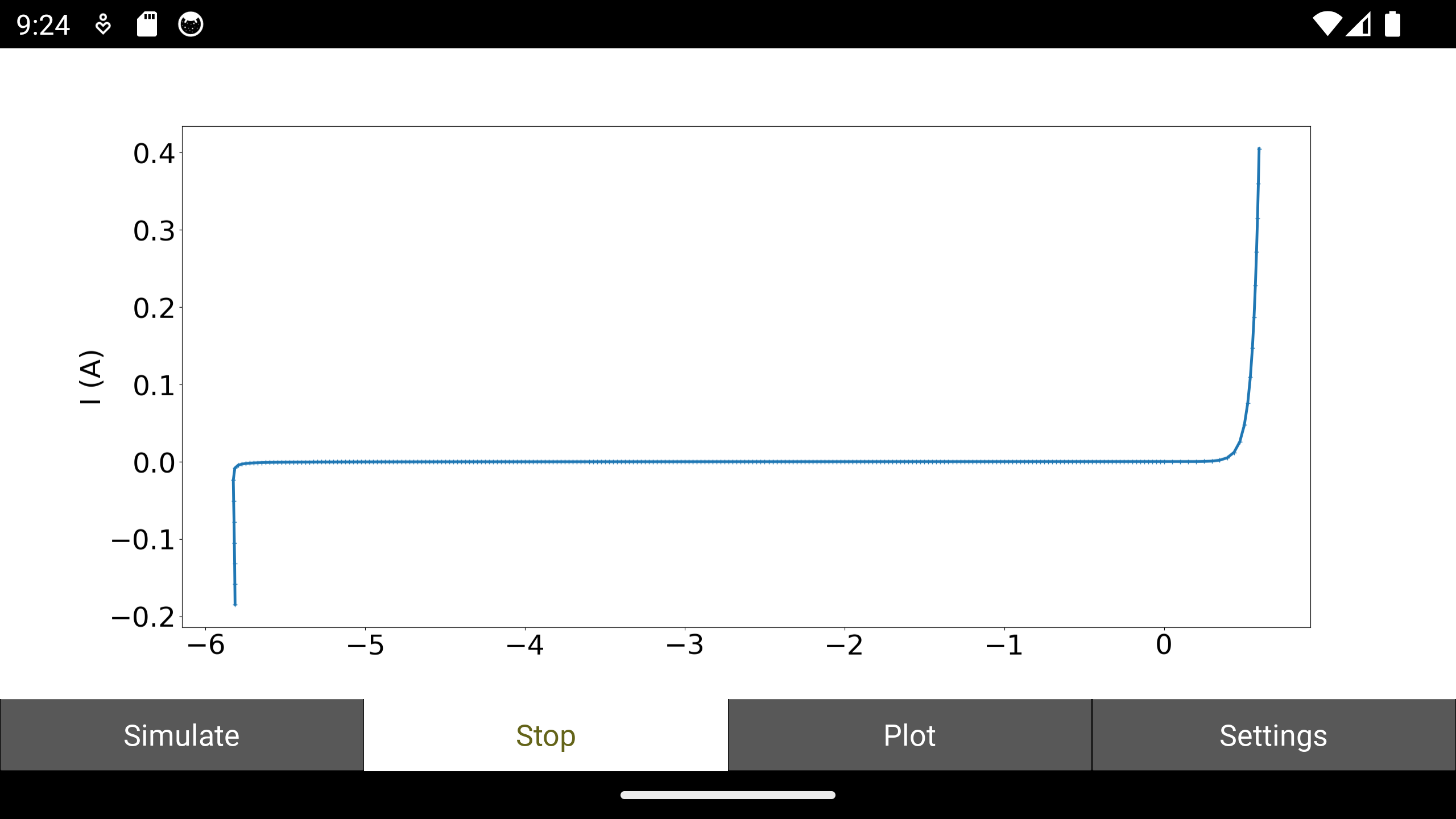
DEVSIM as TCAD mobile app

DEVSIM: TCAD mobile app


Now through January 18, 2024, the TCAD app is free for download. After this, you will be entitled to any free future updates [read more...]

  • App is renamed to “TCAD app”
  • Impact ionization model added
  • Menus updated
  • Easier plot navigation
  • Series resistance available to aid in impact ionization model results
  • Stop simulation and keep partial results to stop long-running simulation early

Get it on Google Play Download on the App Store