May 5, 2020

[paper] Two Transistors Voltage-Measurement-Based Test Structure for Fast MOSFET Device Mismatch Characterization

J. P. M. Brito and S. Bampi
Two Transistors Voltage-Measurement-Based Test Structure 
for Fast MOSFET Device Mismatch Characterization
IEEE Transactions on Semiconductor Manufacturing
doi: 10.1109/TSM.2020.2988095

Abstract - This work presents a test structure targeted to measure MOSFET mismatches with a fast method. It relies on two single-spot voltage measurements in order to extract VTH and β/β separately. The new methodology gives a theoretical increase in the measurement speed of 30x (23.17x in practice). The coefficient of determination (R2) of the linear regression analysis is used to compare standalone transistor measurements against the new proposed methodology. The correlation in the data demonstrates values not less than 0.94 (R2≥ 0.94). The test structure can reproduce parameter correlations, and it is capable of extracting MOSFET mismatch design parameters, such as Pelgrom’s AVTH, with an error of 2% and Aβ, with a negligible error. The experimental data presented herein are taken from measurements in prototypes fabricated in a 65nm CMOS bulk process. The whole circuit is composed of 16 2D addressable DUT device matrices, each having 256 same-size closely-placed MOSFET devices, totaling 4,096 MOS devices used in single-type (NMOS) transistor array. 

URL: https://ieeexplore.ieee.org/stamp/stamp.jsp?tp=&arnumber=9068274&isnumber=5159394

[paper] reached 2000 reads at ResearchGate


Grabiński, Władysław, Daniel Tomaszewski, Laurent Lemaitre, and Andrzej Jakubowski
Standardization of the compact model coding: non-fully depleted SOI MOSFET example
Journal of Telecommunications and Information Technology (2005): 135-141.

Abstract - The initiative to standardize compact (SPICE-like) modelling has recently gained momentum in the semiconduc-tor industry. Some of the important issues of the compact modelling must be addressed, such as accuracy, testing, avail-ability, version control, verification and validation. Most com-pact models developed in the past did not account for these key issues which are of highest importance when introducing a new compact model to the semiconductor industry in par-ticular going beyond the ITRS roadmap technological 100 nm node. An important application for non-fully depleted SOI technology is high performance microprocessors, other high speed logic chips, as well as analogue RF circuits. The IC de-sign process requires a compact model that describes in detail the electrical characteristics of SOI MOSFET transistors. In this paper a non-fully depleted SOI MOSFET model and its Verilog-AMS description will be presented. 

Fig: Approximation of the distribution of currents components
in the non-fully depleted SOI MOSFET.  

Keywords: Verilog-AMS, compact model coding, SOI MOSFET.

References:
  1. ITRS Roadmap Update, 2003, http://www.public.itrs.net
  2. Open Verilog International, "Verilog-AMS, Language Reference Manual", Version 1.9, 1999, http://www.accellera.org/
  3. D. Tomaszewski, "Consistent DC and AC models of non-fully depleted SOI MOSFETS in strong inversion", in Proc. 9th Int. Conf. Mix.-Sig. Des. Integr. Cir. Syst. MIXDES, Wrocław, Poland, 2002, pp. 111-114.
  4. L. Lemaitre, C. McAndrew, and S. Hamm, "ADMS - automatic device model synthesizer", in Proc. IEEE CICC 2002, Florida, USA, 2002, pp. 27-30.
  5. J. R. Hauser, "Small signal properties of field effect devices", IEEE Trans. Electron Dev., vol. 12, pp. 605-618, 1965.
  6. D. Tomaszewski, "A small-signal model of SOI MOSFETs capacitances". Ph.D. thesis, Institute of Electron Technology, Warsaw, 1998.
  7. L. Lemaitre, W. Grabiński, and C. McAndrew, "Compact device modeling using Verilog-A and ADMS", in Proc. 9th Int. Conf. Mix.-Sig. Des. Integr. Cir. Syst. MIXDES, Wrocław, Poland, 2002, pp. 59-62.
  8. C. Lallement, F. Pecheux, and W. Grabiński, "High level description of thermodynamical effects in the EKV 2.6 most model", in Proc. 9th Int. Conf. Mix.-Sig. Des. Integr. Cir. Syst. MIXDES, Wrocław, Poland, 2002, pp. 45-50.

[paper] Memory Technology – A Primer for Material Scientists.

Schenk, Tony, Milan Pesic, Stefan Slesazeck, Uwe Schroeder, and Thomas Mikolajick
Memory Technology–A Primer for Material Scientists
Reports on Progress in Physics (2020)

Abstract - From our own experience in the group, we know that there is quite a gap to bridge between scientists focused on basic material research and their counterparts in a close-to-application community focused on identifying and solving final technological and engineering challenges. In this review, we try to provide an easy-to-grasp introduction to the field of memory technology for materials scientists. As an understanding of the big picture is vital, we first provide an overview about the development and architecture of memories as part of a computer and point out some basic limitations that all memories are subject to. As any new technology has to compete with mature existing solutions on the market, today's mainstream memories are explained and the need for future solutions is highlighted. The most prominent contenders in the field of emerging memories are introduced and major challenges on their way to commercialization are elucidated. Based on these discussions, we derive some predictions for the memory market to conclude the paper.

TABLE OF CONTENTS
1. INTRODUCTION
2. OVERVIEW AND BASIC LIMITATIONS
3. COMMERCIALLY AVAILABLE MAINSTREAM MEMORIES

3.1. Static and Dynamic Random Access Memory (SRAM/DRAM)
3.2. Flash Memory and Solid-State Drive (SSD)
3.3. Magnetic Hard Disk Drives (HDD) and Magnetic Tapes
3.4. Outlook: Market Trends and Drivers
4. EMERGING MEMORIES
4.1. Resistance-based Read-out: Memory Concepts and Basic Considerations
4.2. Anion migration or valence change memory (VCM)
4.3. Cation migration or electrochemical metallization memory (ECM)
4.4. Phase change memory (PCM)
4.5. Magnetoresistive memory (MRM)
4.6. Ferroelectric Memory (FEM)
4.7. Miscellaneous
5. SUMMARY AND CONCLUSION

FIG: Evolution of the mainstream solutions for the respective memories classes. The introduction of Flash memory partially bridged a technology gap around the year 2009. Today, two types of so-called storage-class memories – a memory-type SCM (SCM 1) and a storage-type SCM (SCM 2) – were proposed to overcome the memory gap. NAND flash already fulfills the role of a mainstream SCM 2. For SCM 1, 3D XPoint could be a promising candidate, but is not a dominant mainstream memory. In future, we will likely see different types of SCMs and NV-RAM with different specifications as required by the respective application – because in the end, the overall system cost decides about the choice of the memory.

May 4, 2020

[paper] Benchmark Tests for MOSFET Thermal Noise Models

Scholten A.J., Smit G.D.J., Pijper R.M.T., Tiemeijer L.F.
Benchmark Tests for MOSFET Thermal Noise Models
In: Grasser T. (eds) Noise in Nanoscale Semiconductor Devices. Springer, Cham

Abstract - In today’s semiconductor industry, many traditional integrated device manufacturers (IDMs) are moving away from chip manufacturing, and transforming into fabless companies that use foundry services for manufacturing their ICs. This is especially true in the field of advanced CMOS technologies. In these companies-under-transformation, the work of the modeling engineer is changing: instead of building models from scratch themselves, most companies choose to use the modeling packages that are delivered by the foundries. There are two reasons to be skeptical about RF noise models. First, measurement of noise, and RF noise in particular, is a difficult and specialist topic. One should not take for granted that every company has the required expertise to carry out this task successfully. A second reason to check RF noise models is that the most popular compact MOSFET models are BSIM4 [1] and BSIMBULK [2], which are not particularly strong and certainly not predictive when it comes to RF noise. As a consequence, the work of the modeling engineer is changing from model creation to model verification.

Tab: Overview of benchmark tests for thermal noise
#No
Bias
Length
Quantity
Test
Remark
#1
VDS = 0V
All
SID
γ = 1

#2
VDS = 0 V
All
SIG
β = 5/12

#3
VDS = 0 V
All
c
c = 0
In the limit f ↓ 0 Hz
#4
Weak Inv
All
SID
F = 1
Disregard SIG contributions from gate to drain
#5
Saturation
Long
SID
γ = 2/3

#6
Saturation
Long
SIG
β = 4/3

#7
Saturation
Long
c
c = 0.4j

#8
Saturation
Short
SID
γ enhancement
Switch off gate resistance
#9
Saturation
All
SID
γ D,NMOS ≥ γ D,PMOS
Switch off gate resistance
#10
Saturation
All
SID
Different Vth flavors should nearly coincide
When plotted against ID


First Online: 27 April 2020
DOI: 10.1007/978-3-030-37500-3_20

Ref: 
[1] N. Paydavosi, T.H. Morshed, D.D. Lu, W. Yang, M.V. Dunga, X. Xi, J. He, W. Liu, K.M. Cao, X. Jin, J.J. Ou, M. Chan, A.M. Niknejad, C. Hu, BSIM4v4.8.0 MOSFET Model - User’s Manual. [Online]. Available: http://bsim.berkeley.edu/models/bsim4/
[2] H. Agarwal, C. Gupta, H.-L. Chang, S. Khandelwal, J.P. Duarte, Y.S. Chauhan, S. Salahuddin, C. Hu, BSIM-BULK106.2.0 MOSFET Compact Model - Technical Manual. [Online]. Available: http://bsim.berkeley.edu/models/bsimbulk/

[paper] DHBT with Record ft of 813 GHz

Y. Shiratori, T. Hoshi and H. Matsuzaki,
InGaP/GaAsSb/InGaAsSb/InP Double Heterojunction Bipolar Transistors
With Record ft of 813 GHz
IEEE EDL vol. 41, no. 5, pp. 697-700, May 2020
doi: 10.1109/LED.2020.2982497

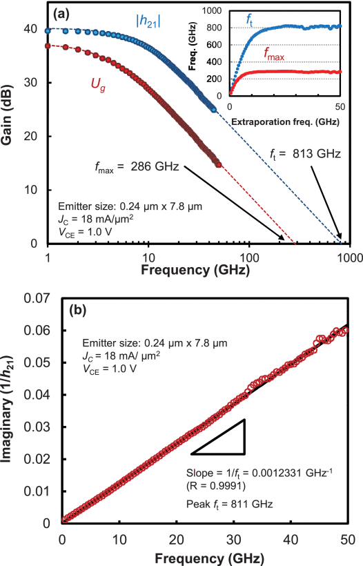
Abstract - We fabricated InGaP/GaAsSb/InGaAsSb/InP double heterojunction bipolar transistors (DHBTs) with an aggressive lateral and vertical scaling technology to improve the current gain cutoff frequency (fT) further. A 13-nm-thick GaAsSb/InGaAsSb base and a 40-nm-thick InP collector are used to reduce electron transit time. In addition, the width of the base electrode on each side of the emitter is reduced to about 0.05µm to suppress increases in parasitic collector capacitance. A fabricated DHBT with the emitter size of 0.24µm×7.8 µm exhibits maximum differential current gain of ∼95 and collector-emitter breakdown voltage of 2.6V. At a collector current density of 18 mA/µm2, the DHBT exhibits fT of 813 GHz, which is the highest among all types of transistors measured at a room temperature.
Fig: (a) Current gain ( |h21| ) and Mason’s unilateral power gain (Ug ) of the DHBT as a function of frequency. JC and VCE are 18 mA/μm2 and 1.0 V, respectively. ft and fmax are extrapolated by single-pole fitting. Inset: frequency dependence of extrapolating ft and fmax . (b) Gummel’s ft extraction (imaginary part of 1/h21 as a function of frequency). The red circles and black line show experimental data and a linear fitting, respectively.

URL: https://ieeexplore.ieee.org/stamp/stamp.jsp?tp=&arnumber=9044299&isnumber=9079222