Feb 27, 2021

Feb 26, 2021

[DAY 2] 1st Asia/South Pacific MOS-AK Workshop

Arbeitskreis Modellierung von Systemen und Parameterextraktion
Modeling of Systems and Parameter Extraction Working Group
1st Asia/South Pacific MOS-AK Workshop
(virtual/online) FEB. 25-26, 2021

Day2: FEB.26
Session C Chair: Sadayuki Yoshitomi, Kioxia (J)

[8] eSim: An open source CAD software for circuit simulation
Kannan Moudgalya
IIT Bombay (IN)

[9] A modular approach to next generation Qucs
Felix Salfelder and Mike Brinson
QUCS Team; Centre for Communications Technology, London Metropolitan University (UK)

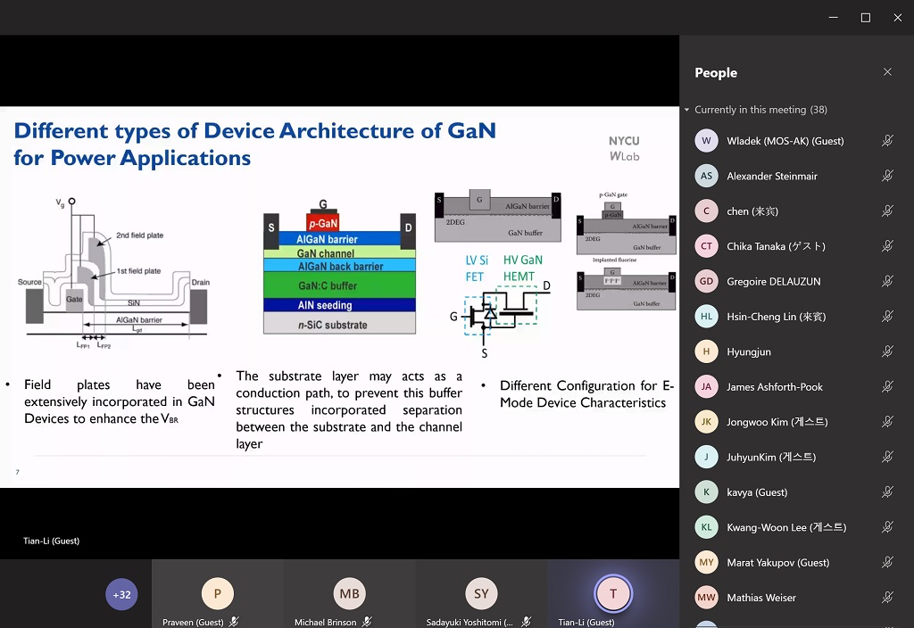
[12] Machine learning-based approach to model and analyze GaN power devices
Tian-Li Wu
National Yang Ming Chiao Tung University, Taiwan (TW)

[11] TCAD-inspired compact modeling approach
Sung-Min Hong and Kwang-Woon Lee
Gwangju GIST (KR)

Session D Chair: Sheikh Aamir Ahsan, NIT Srinagar (IN)
[10] An Innovative Technique for Ultrafast Carrier Dynamics and THz Conductivities of Semiconductor Nanomaterials
Praveen Kr. Saxena and Fanish Kr. Gupta
Tech Next Lab, Lucknow (IN)

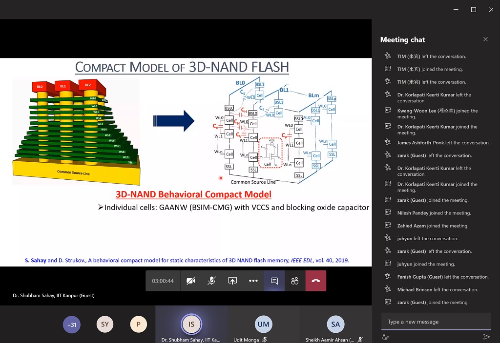
[13] Compact Modeling of 3D NAND Flash Memory for Diverse Unconventional Analog Applications
Shubham Sahay
IIT Kanpur (IN)

[14] Steep Subthreshold Slope PN-Body Tied SOI-FET for Ultralow Power LSI, Sensor, and Neuromorphic Chip
Takayuki Mori and Jiro Ida
Kanazawa Institute of Technology, Nonoichi (J)

[Pic] Group photo of selected MOS-AK participants attending 2nd Day of the workshop


[DAY 1] 1st Asia/South Pacific MOS-AK Workshop

Arbeitskreis Modellierung von Systemen und Parameterextraktion
Modeling of Systems and Parameter Extraction Working Group
1st Asia/South Pacific MOS-AK Workshop
(virtual/online) FEB. 25-26, 2021

DAY 1: FEB. 25, 2021
Session A Chair: Usha Gogineni, ams AG, Hyderabad (IN)

[1] New Insights in Low Frequency Noise Characteristics in PE-BJTs
Peijian Zhang and Ma Long
Science and Technology on Analog Integrated Circuit Laboratory; WHU (CN), Keysight Technologies (US)

[2] Direct white noise characterization of short-channel MOSFETs
K. Ohmori and S. Amakawa
DeviceLab, Tsukuba (J)

[3] SPICE Modeling of 2D-material based FETs with Schottky-barrier contacts
Sheikh Aamir Ahsan
Nanoelectronics Research and Development Group, NIT Srinagar, Jammu and Kashmir (IN)


[4] Physics-based model of SiC MOSFETs including high voltage and current regions
Sourabh Khandelwal, Cristino Salcines, and Ingmar Kallfass
Macquarie University Sydney (AU), University of Stuttgart (D)

Session B Chair: Daniel Tomaszewski, IMiF, Warszaw (PL)
[5] Compact Modeling for Gate-All-Around FET Technology
Avirup Dasgupta
IIT Roorkee (IN)


[6] BSIM-HV: Advanced High Voltage MOSFET Compact Model
Harshit Agarwal
IIT Jodhpur (IN)

[7] ASCENT+ Transnational Access for the nanoelectronics
Georgios Fagas
Tyndall (IE)

[Pic] Group photo of selected MOS-AK participants attending 1st Day of the workshop

[https://t.co/42ahdl8o1h] Study Captures #India's Rise in #Nanoelectronics Research https://t.co/xGqsmBiKKa #semi https://t.co/XNnB7RP3Fn


from Twitter https://twitter.com/wladek60

February 26, 2021 at 02:32PM
via IFTTT

President Biden signed an executive order Wednesday addressing growing concern over a global semiconductor shortage hampering the production of goods like automobiles and smartphones. https://t.co/JGZVSGVeSF #semi https://t.co/vWAg7EaYW8


from Twitter https://twitter.com/wladek60

February 26, 2021 at 02:16PM
via IFTTT