Jul 23, 2019

[paper] A Surface-Potential-Based Analytical I-V Model of Full-Depletion Single-Gate SOI MOSFETs

1
Department of Electrical and Electronic Teaching, 
College of Information Science and Engineering, 
Huaqiao University, Xiamen 361021, China

2
Department of Electronic Engineering, Jinan University, Guangzhou 510632, China
*
Correspondence: yufei_jnu@126.com; Tel.: +86-0592-6162-385
These two authors contributed equally to this work.

Received: 10 May 2019 / Accepted: 12 June 2019 / Published: 14 July 2019
Electronics 20198(7), 785; https://doi.org/10.3390/electronics8070785

Abstract

: 
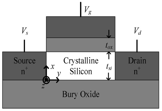
A surface-potential-based analytical I-V model of single-gate (SG) silicon-on-insulator (SOI) MOSFETs in full-depletion (FD) mode is proposed and compared with numerical data and Khandelwal’s experimental results. An explicit calculation scheme of surface potential, processing high computation accuracy and efficiency, is demonstrated according to the derivation of the coupling relation between surface potential and back-channel potential. The maximum absolute error decreases into 10−7 V scale, and computation efficiency is improved substantially compared with numerical iteration. Depending on the surface potential, the drain current is derived in closed-form and validated by Khandelwal’s experimental data. High computation accuracy and efficiency suggest that this analytical I-V model displays great promise for SOI device optimizations and circuit simulations.

Keywords:
 silicon-on-insulator MOSFETs; surface potential; back-channel potential; full-depletion; analytical I-V model
Figure 1. x-y cross section of silicon-on-insulator (SOI) MOSFETs.

Jul 12, 2019

IEEE ICECS 2019 paper submission deadline

ICECS 2019 paper deadline submission is approaching fast: July 15th, 2019

Please distribute this reminder to possible contributors and interested researchers and colleagues. Topics of interest include but are not limited to:

• Analog/mixed-signal/RF circuits
• Biomedical and Bio-Inspired Circuits and Systems
• EDA, Test and Reliability
• Digital circuits and systems
• Linear and Non-linear Circuits
• Low-Power Low-Voltage Design
• Microsystems
• Neural networks, Machine and Deep Learning
• Sensors and Sensing Systems
• Signal Processing, Image and Video
• VLSI Systems and Applications

The technical committee invites authors to submit 4-page papers in standard IEEE double-column format, including references, figures and tables, to clearly present the work, methods, originality, significance and applications of the techniques discussed.

Maurizio Valle; IEEE ICECS 2019 General Chair
https://www.ieee-icecs2019.org/

Jul 8, 2019

Leti Workshop at SISPAD 2019

Leti is pleased to invite you to attend our ‘Advanced Simulations for Emerging Non-Volatile Memory Technologies’ seminar, which is organized as an official satellite event of the 2019 IEEE SISPAD Conference (http://www.sispad2019.org). By the proposed seminar, we will emphasize how simulation and modeling support memory technology developments and device behavior understanding.

This event will held on Tuesday, September 3rd from 5:00 PM to 7:30 PM, Palazzo di Toppo Wassermann, Università degli Studi di Udine, Udine, Italy (i.e. at the SISPAD 2019 conference location).
PROGRAM

  • Welcome and Introduction – T. Poiroux
  • Innovative non-volatile memory technologies: a revolution for the storage towards a memory that thinks – G. Navarro
  • Electro-thermal and material simulations for PCM – O. Cueto
  • Multiphase field method for the simulation of the complex phase changes in PCM – R. Bayle
  • Invited talk: Self-consistent TCAD simulation of chemical reactions within electronic devices. Application to CBRAM and OxRAM – Silvaco
  • Networking cocktail

Registration is free but, due to limited seats, please register just sending an email to thierry.poiroux@cea.fr and sebastien.martinie@cea.fr.

Feel free to share this invite with your colleagues !

Jun 17, 2019

[open source paper] Open-source circuit simulation tools for RF compact semiconductor device modelling

Wladek Grabinski (editor), Mike Brinson, Paolo Nenzi, Francesco Lannutti, Nikolaos Makris, Angelos Antonopoulos and Matthias Bucher
September 2014
DOI: 10.1002/jnm.1973

SUMMARY: MOS-AK is a European, independent compact modelling forum created by a group of engineers, researchers and compact modelling enthusiasts to promote advanced compact modelling techniques and model standardization using high level behavioral modelling languages such as VHDL-AMS and Verilog-A. This invited paper summarizes recent MOS-AK open source compact model standardization activities and presents advanced topics in MOSEFT modelling, focusing in particular on analogue/RF applications. The paper discusses links between compact models and design methodologies, finally introducing elements of compact model standardization. The open source CAD tools: Qucs, QucsStudio and ngspice all support Verilog-A as a hardware description language for compact model standardization. Latter sections of this paper describe a Verilog-A implementation of the EKV3 MOS transistor model. Additionally, the simulated  RF model performance is evaluated and compared with experimental results for 90nm CMOS technology. 

KEYWORDS: CAD; GNU; Qucs; QucsStudio; ngspice; compact modeling; EKV3; RF; MOSFET; Verilog-A