
Oct 15, 2014
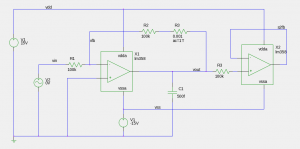
AC and Stability Analysis in NGSPICE
Oct 13, 2014
Wearable Sensing and Computing
Wearable Sensing and Computing
05.11.2014 - 06.11.2014
EPFL Lausanne (CH)
COURSE OBJECTIVES
The course main objective is to inform and discuss in great details the latest advancements in low power sensing technology, energy harvesting and their heterogeneous integration for wearable smart system applications. Technological roadmaps of performance and future evolutions will be presented. The low power wireless communications are discussed from the point of view of existing standards and challenges for reducing the energy per communicated bit. Another objective is to detail some key future applications for wearable sensing and computing with main emphasis on: (1) medical Diagnostics, monitoring and prevention and (2) sports, fitness and activity monitoring applications. We analyze the benefits of autonomous smart system technology from many different points of view, including that of the individual, the physician, health care management, and society in general. We provide a rationale on the role of such technology as a component of the care cycle and the changes it can induce by reinforcing preventive strategies.
AGENDA on-line
Day 1 (09:00 – 17:00):
- Introduction to wearable technology and energy efficient functions for autonomous smart systems
- Energy efficient computing technologies and their importance for wearable applications:
- Wearable low power sensor technology trends
- Wearable low power communications technologies
- Wearable energy harvesting technology trends
Day 2 (09:00 – 17:00):
- Heterogeneous integration: solutions, roadmaps and trends for wearables
- Context-driven embodiments by wearable systems and related applications and services
- Market Trends for Mobile and Wearable Technology
- Wearable autonomous smart systems: Applications to Medical Diagnostics, Monitoring and Prevention Paradigms using Feedback Loops
- Wearable Technology – Sports, Fitness and Activity Monitoring Applications
Course registration on-line
Oct 7, 2014
[mos-ak] 7th International MOS-AK Workshop; December 12, 2014 at Berkeley
7th International MOS-AK Workshop
Berkeley Friday, Dec. 12, 2014
Announcement and Call for Papers
Together with the MOS-AK Workshop Scientific Program Coordinators Larry Nagel and Andrei Vladimirescu as well as Extended MOS-AK TPC Committee, we have pleasure to invite to the 7th consecutive International MOS-AK Workshop which will be held at Berkeley, California, USA, in the IEDM Conference and CMC Meeting timeframe. The event is organized with aims to strengthen a network and discussion forum among experts in the field, enhance open platform for information exchange related to compact/Spice modeling and Verilog-A standardization, bring people in the compact modeling field together, as well as obtain feedback from technology developers, circuit designers, and CAD/EDA tool vendors.
Venue:
Room 540 in Cory HallEECS DepartmentUniversity of California, Berkeley
Important Dates:
Call for Papers - September 20142nd Announcement - October 2014Final Workshop Program - November. 2014MOS-AK Workshop - Friday, Dec. 12, 201408:30 - 09:00 - On-site Registration09:00 - 11:00 - Morning MOS-AK Session11:00 - 12:00 - CM Standardization Panel12:00 - 13:00 - Lunch13:00 - 16:00 - Afternoon MOS-AK Session
- Advances in semiconductor technologies and processing
- Compact Modeling (CM) of the electron devices
- Verilog-A language for CM standardization
- New CM techniques and extraction software
- Open Source TCAD/EDA modeling and simulation
- CM of passive, active, sensors and actuators
- Emerging Devices, CMOS and SOI-based memory cells
- Microwave, RF device modeling, high voltage device modeling
- Nanoscale CMOS devices and circuits
- Technology R&D, DFY, DFT and IC Designs
- Foundry/Fabless Interface Strategies
Authors should submit an abstract using on-line MOS-AK submission form (any related inquiries can be sent to abstracts@mos-ak.org)
http://www.mos-ak.org/berkeley_2014/abstracts.php
On-line free workshop registration:
http://www.mos-ak.org/berkeley_2014/registration.php
Postworkshop publications:
Selected best MOS-AK technical presentation will be recommended for further publication in a special issue of the International Journal of High Speed Electronics and Systems
Extended MOS-AK/GSA Committee
WG06102014
You received this message because you are subscribed to the Google Groups "mos-ak" group.
To unsubscribe from this group and stop receiving emails from it, send an email to mos-ak+unsubscribe@googlegroups.com.
To post to this group, send email to mos-ak@googlegroups.com.
Visit this group at http://groups.google.com/group/mos-ak.
For more options, visit https://groups.google.com/d/optout.
Sep 11, 2014
Open Ph D scholarship on semiconductor device modeling
We offer one scholarship for a Ph D student position in the Department of Electronic Engineering in theUniversitat Rovira i Virgili (URV), in Tarragona , Spain
The duration of the grant will be for three years. The monthly salary will be about 1000 Euro/month. The position will start in January 2014.
The candidate should have a Bachelor and Master degree in Electrical Engineering, Electronic Engineering, Telecommunication Engineering or Physics. A good background in Semiconductor Physics, Semiconductor Devices, or Integrated Circuit Design will be highly appreciated.
The work to be done by the candidate will be focused on the development of new techniques of characterization and modeling of novel advanced semiconductor devices, in particular III-V devices. It will be related to European and national projects in which the hosting group (the so-called NEPHOS group) participates. One recent European Union project coordinated by our NEPHOS group is COMON (COmpact MOdelling Network)
The work to be done by the candidate will be focused on the development of new techniques of characterization and modeling of novel advanced semiconductor devices, in particular III-V devices. It will be related to European and national projects in which the hosting group (the so-called NEPHOS group) participates. One recent European Union project coordinated by our NEPHOS group is COMON (COmpact MOdelling Network)
The NEPHOS group at URV is one of the most powerful teams in Europe in the area of compact modeling of semiconductor devices.
Required documents for applicants
Applicants are required to send to the address specified below the following documents (in English or Spanish):
Applicants are required to send to the address specified below the following documents (in English or Spanish):
1) a full Curriculum Vitae (as complete as possible) with passport number
2) Copy of their diploma
3) copy of their passport
4) Academic certificate including their marks (it is important that the number of hours or credits of each subject appears) for the subjects studied when pursuing Bachelor Degree and Master degree. It is also very important that the document specifies what is the minimum mark for passing a given subject and what is the maximum mark that can be awarded.
Candidates are requested to send their documents by e-mail to:
Prof. Benjamin IñiguezDepartment of Electronic, Electrical and Automatic Control Engineering
Universitat Rovira i Virgili (URV)
Avinguda Països Catalans, 26
43007Tarragona Spain
43007
Deadline:
You can contact Prof. Benjamin Iñiguez (Benjamin.Iniguez@gmail.com) for more information
Aug 14, 2014
[mos-ak] [Final Program] 12th MOS-AK Workshop at the ESSDERC/ESSCIRC Conference in Venice
Autumn MOS-AK Workshop in Venice
Together with the MOS-AK Workshop Scientific Program Coordinators Larry Nagel and Andrei Vladimirescu as well as Extended MOS-AK TPC Committee, we have pleasure to invite to the 12th consecutive MOS-AK at the ESSDERC/ESSCIRC Conference.
Venue:
Palazzo del CasinòLungomare Marconi, 3030126 Venice Lido, Italy
MOS-AK Workshop Online Registration
MOS-AK Workshop Program
08:30-08:50 On-site Registration
08:30-08:50 Morning Session: Open Source CAD/EDA Tools
Is It Time To Rethink the SPICE Input "Language"?
Larry NagelOmega Enterprises Consulting (USA)
Parallel Circuit Simulation: How Good Can It Get?
Andrei VladimirescuISEP (FR); UCB (USA)
CUSPICE: The revolutionary NGSPICE on CUDA Platforms
Francesco LannuttiSapienza University of Rome (I)
10:30-11:00 Coffee break
Circuit Simulation Update: GPU Progress; Electrothermal Cosimulation
Rick PooreKeysight Technologies (USA)
QUCS Roadmap
Mike BrinsonQUCS Development (EU)
12:30-13:30 Lunch
13:30-16:30 Afternoon MOS-AK Session: Device Level SPICE/Verilog-A Modeling
Total Virtual Fabrication of Advanced CMOS Devices and Processing
W. Clark, M. Hargrove, G. Schropfer, D. FriedCoventor (F)
Performance Comparison of Hall Effect Sensors Obtained by Regular Bulk or SOI CMOS Technology
Maria-Alexandra PaunUniversity of Cambridge, (UK)
RF Characterization and Modeling of Nanoscale MOSFET from Weak to Strong Inversion
Maria-Anna Chalkiadaki and Christian EnzEPFL STI IMT ICLAB (CH)
THz Compact Modeling
Michael ShurRensselaer Polytechnic Institute, NY, (USA)
Compact Modeling of Junctionless Cylindrical Nanowires
Benjamin IniguezURV, (SP)
Comparative Analysis of SOI/SOS MOSFET SPICE Models with Account for Radiation Effects
Konstantin Petrosyants(1), Igor Kharitonov (1), Lev Sambursky (1,2)(1) MIEM HSE (RU), (2) IPPM RAS (RU)
16:30 End of the MOS-AK Workshop
Postworkshop publications:
selected best MOS-AK technical presentation will be recommended for further publication in a special issue of the International Journal of High Speed Electronics and Systems
You received this message because you are subscribed to the Google Groups "mos-ak" group.
To unsubscribe from this group and stop receiving emails from it, send an email to mos-ak+unsubscribe@googlegroups.com.
To post to this group, send email to mos-ak@googlegroups.com.
Visit this group at http://groups.google.com/group/mos-ak.
For more options, visit https://groups.google.com/d/optout.
Aug 11, 2014
Dr. Jindal has been nominated for the Delegate-Elect/Director-Elect 2015
Dr. Renuka Jindal is Professor of Electrical and Computer Engineering at the University of Louisiana at Lafayette, LA, USA since 2002. His research and teaching interests lie in the theory and practice of random processes applicable to a wide variety of phenomena in electronic and photonic devices and circuits, lightwave and wireless communications systems and biological organs. Dr. Jindal was elected Fellow of IEEE in 1991 for his seminal work reducing MOSFET noise by almost an order of magnitude for analog and RF applications. He is also a recipient of the IEEE 3rd Millennium medal. For last four decades of his dual career in industry and academia, Dr. Jindal rose through the ranks as Editor, Editor-in-Chief, VP of Publications, and as EDS President in 2010- 2011. As President he formulated the vision and mission of EDS enhancing member benefits launching a plethora of initiatives reversing the decline in EDS membership. A partial list of his accomplishments is given below:
- Brought together 6 societies and 1 council to launch highly successful IEEE Journal of Photovoltaics mushrooming IEEE’s share in the PV space http://ieeexplore.ieee.org/stamp/stamp.jsp?tp=&arnumber=6055242
- Launched EDS webinar series serving the practicing engineers; now considered a best practice in IEEE http://eds.ieee.org/webinars.html
- Launched the 1st EDS OPEN ACCESS Journal J-EDS http://ieeexplore.ieee.org/stamp/stamp.jsp?tp=&arnumber=6471856
- Founded QuestEDS for members to get authoritative answers to technical questions within 2 weeks http://eds.ieee.org/questeds/why-questeds.html
- Founded the EDS Celebrated Member program to honor EDS Nobel Laureates and other luminaries. http://eds.ieee.org/celebrated-members.html
- Mentored the launch of a high-school outreach program (EDS-ETC) across United States and abroad http://eds.ieee.org/the-eds-etc-program.html
- As chapter partner, for over 15 years, stimulated a spectacular growth of EDS chapters in South Asia from one to 19 serving Division I.
As Senior-Past President of EDS Dr. Jindal is still very much engaged with IEEE. Recently, Dr. Jindal has been nominated by IEEE Division I to run for the Delegate-Elect/Director-Elect 2015 position in the upcoming IEEE elections. The electorate consists of members of three societies i.e. Electron Devices (ED), Solid-State Circuits (SSC) and Circuits and Systems (CAS). The slate consists of three candidates one from each of these societies.
On his behalf, I suggest to contact your colleagues in IEEE regions 1-10 for his support since IEEE ballots will be out by August 15.
Jul 30, 2014
Semiconductor Devices Characterization Seminar
Technical Seminars addressing the challenges of CMOS, Power and RF
semiconductor device measurement and modeling
Agilent and it´s 25 collaborative partners invite you to attend this complimentary technical seminar on characterization and modeling of semiconductor devices. Two tracks in parallel will address the needs for:
To obtain the detail agenda of the nearest session, please select one of the locations below.

- Small scale silicon industry
- Power silicon industry and RF Power
- Live demonstration of GaN device characterization flow: DC I-V characteristic extraction, RF Power measurement, Spice models creation for further usage in design stage.
- Accurate and repeatable on-the-wafer device extraction – Cascade Microtech
- DC characterization for emerging nano-technologies
- Flicker Noise and Random Telegraph Noise
- Spice model libraries optimization for dedicated application
- High Power Devices measurement
- III-V devices spice model (DynaFET)
- Nonlinear Component characterization
- Non-50ohm Load Pull solution – Maury
To obtain the detail agenda of the nearest session, please select one of the locations below.
| Country | City | Date | More Information |
|---|---|---|---|
| FR | Grenoble | 18 September 2014 | Register here |
| FI | Helsinki | 23 September 2014 | Register here |
| DE | Munich | 30 September 2014 | Register here |
| DE | Dresden | 2 October 2014 | Register here |
| CH | Lausanne | 14 October 2014 | Register here |
| BE | Leuven | 16 October 2014 | Register here |
| NL | Eindhoven | 17 October 2014 | Register here |
| SW | Goteborg | 28 October 2014 | Register here |
| UK | Cambridge | 30 October 2014 | Register here |
| FR | Les Ulis | 6 November 2014 | Register here |
Subscribe to:
Posts (Atom)