May 24, 2024

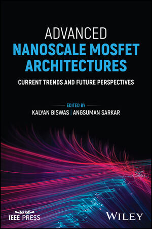
[book] Advanced Nanoscale MOSFET Architectures

Advanced Nanoscale MOSFET Architectures:
Current Trends and Future Perspectives
Kalyan Biswas, Angsuman Sarkar
John Wiley & Sons - Technology & Engineering (2024) 336 pages
ISBN: 978-1-394-18894-9

Comprehensive reference on the fundamental principles and basic physics dictating metal–oxide–semiconductor field-effect transistor (MOSFET) operation. Advanced Nanoscale MOSFET Architectures provides an in-depth review of modern metal–oxide–semiconductor field-effect transistor (MOSFET) device technologies and advancements, with information on their operation, various architectures, fabrication, materials, modeling and simulation methods, circuit applications, and other aspects related to nanoscale MOSFET technology. The text begins with an introduction to the foundational technology before moving on to describe challenges associated with the scaling of nanoscale devices. Other topics covered include device physics and operation, strain engineering for highly scaled MOSFETs, tunnel FET, graphene based field effect transistors, and more. The text also compares silicon bulk and devices, nanosheet transistors and introduces low-power circuit design using advanced MOSFETs.

Table of Contents:
[1] Emerging MOSFET Technologies; pp. 1
Kalyan Biswas and Angsuman Sarkar
[2] MOSFET: Device Physics and Operation; pp. 15
Ruthramurthy Balachandran, Savitesh M. Sharma, and Avtar Singh
[3] High-k Dielectrics in Next Generation VLSI/Mixed Signal Circuits; pp. 47
Asutosh Srivastava
[4] Consequential Effects of Trap Charges on Dielectric Defects for MU-G FET; pp. 61
Annada S. Lenka and Prasanna K. Sabu
[5] Strain Engineering for Highly Scaled MOSFETs; pp. 85
Chinmay K. Maiti, Taraprasanna Dash, Jhansirani Jena, and Eleena Mohapatra
[6] TCAD Analysis of Linearity Performance on Modified Ferroelectric Layer in FET Device with Spacer; pp. 113
Yash Pathak, Kajal Verma, Bansi Dhar Malhotra, and Rishu Chauzar
[7] Electrically Doped Nano Devices: A First Principle Paradigm; pp. 125
Debarato D. Ray, Pradipta Roy, and Debashis De
[8] Tunnel FET: Principles and Operations; pp. 143
Zahra Ahangari
[9] GaN Devices for Optoelectronics Applications; pp. 175
Nagarajan Mohankumar and Girish S. Mishra
[10] First Principles Theoretical Design on Graphene-Based Field-Effect Transistors; pp. 201
Yoshitaka Fujimoto
[11] Performance Analysis of Nanosheet Transistors for Analog ICs; pp. 221
Yogendra R Pundir, Arvind Bisht, and Pankaj K. Pal
[12] Low-Power Analog Amplifier Design using MOS Transistor in the Weak Inversion Mode; pp. 255
Soumya Pandit and Koyel Mukherjee
[13] Ultra-conductive Junctionless Tunnel FET-based Biosensor with Negative Capacitance; pp. 281
Palasri Dhar, Soumik Poddar, and Sunipa Roy
[14] Conclusion and Future Perspectives; pp. 301
Kalyan Biswas and Anqsuman Sarkar
[INDEX]; pp. 311

[Libre Silicon] Free Semiconductors For Everyone

Libre Silicon aims to take an active role in driving forward the change and reaching the objectives outlined before. Considering the fact that the free and open-source silicon ecosystem is growing explosively since the second half of the 2010s, many of the objectives are addressed already by others. In these cases, Libre Silicon wants to support their effort and adapt their results, without aiming at realizing the same goal differently, thus preventing the fragmentation of the ecosystem. In other topics, however, there is either no progress or the progress is not going in the desirable direction. In these cases, Libre Silicon takes a leading role, using the fullest possible extent of our expertise, commitment and resources. Our focus topics, without particular order, are the following:
  • Develop free technology nodes, including manufacturing recipes, test structures, primitive devices, logic, padrings, analog and other libraries, characterization methodology, and PDK support.
  • Drive the adoption of these nodes, by providing the necessary documentation, consulting and technical support. Libre Silicon also aims to set the example to follow by being early adopters of our own technology nodes, including the provision of actual manufacturing service.
  • Elaborate novel business models to support the emergence of universal and affordable access to semiconductor technologies. This includes, among others, novel manufacturing operation organization concepts, throughput optimization for low-volume or high-volume production, and the introduction of new, connected manufacturing concepts and equipment.
  • Develop novel manufacturing equipment enabling low-volume-capable, high-flexibility manufacturing, with primary focus on maskless lithographic technologies.

In addition to these efforts, Libre Silicon also aims at providing valuable contribution to the efforts of others with shared goals, including:

  • Drive the necessary paradigm shift by advocating for free and open-source silicon solutions in real-life applications
  • Support the education on IC design-related skillset by taking active role in the formation of training materials, supporting and organizing events like Hackathons or workshops and mentoring
  • Support the development of EDA tools by advising on, and contributing to, the development of FOSS IC design software
  • Increase the scope and quality of available free silicon IP libraries by developing our own libraries and contributing to the development of others
Libre Silicon roadmap is the following:
  • Establishment of LibreSilicon Foundation in Europe
  • Finish LS1U technology node (incl. SPICE parameter extraction)
  • Development of ESD protection and pad cell library for LS1U
  • Development of a maskless lithography stepper
  • Tech Demo: LS555 (design, MLL fabrication, testing)
  • Digital cell library for 1u MFS + digital tools (maybe parallel to LS1U/LS555)
  • Tech demo II: 8-bit Arduino-compatible MCU
  • To open Libresilicon Fabrication Service in EU
  • Development of LS130 technology node (incl. MLL capability)
  • Tech demo III: 130nm System-on-Chip
  • Development of sub-100nm technology node (incl. MLL capability)
  • Tech demo IV: SOC made on LibreSilicon runs GNU/Linux
  • Successful tapeout of the Danube with Global Foundries. The first successful tapeout of the new autogenerated process verification wafer Danube River
Contact -> Lebre Silicon

[paper] Półprzewodnikowa rewolucja w domenie open source

Krzysztof Herman and Anna Sojka-Piotrowska
https://bit.ly/IHPOpenPDK
* IHP GmbH – Leibniz Institute for High Performance Microelectronics, Frankfurt (Oder), Niemcy

Abstract: Hasło „open source” kojarzy się większości osób przede wszystkim z oprogramowaniem tworzonym przez pasjonatów informatyki i udostępnianym za darmo ogólnoświatowej społeczności użytkowników. Nie mniej interesująca jest jednak grupa otwartych rozwiązań sprzętowych, czyli open source hardware – mało kto wie, że istnieją już bezpłatne pakiety oprogramowania przeznaczonego do projektowania układów scalonych, w tym nawet układów ASIC o paśmie rzędu setek GHz. Jeszcze większym zaskoczeniem może być fakt, że fabryki półprzewodników otwierają swoje podwoje także dla małych firm, partnerów akademickich, a nawet... odbiorców prywatnych! (czytaj dalej...)

Rys: Zestaw narzędzi open source do projektowania układów analogowych 
z uwzględnieniem pasma RF

Kontakt: dr Krzysztof Herman, dr Anna Sojka-Piotrowska

Ważne linki:

[paper] Rapid MOSFET Threshold Voltage Testing

Michael H. Herman; Trenton T. Nguyen; Ken Wong; Jeff Johnson; Ben Morris
Rapid MOSFET Threshold Voltage Testing
for High Throughput Semiconductor Process Monitoring
2024 IEEE 36th International Conference on Microelectronic Test Structures (ICMTS)
Edinburgh, United Kingdom, 2024, pp. 1-6
doi : 10.1109/ICMTS59902.2024.10520252

* Parametric Test Group, Advantest America, San Jose, CA 95134 United States

Abstract : We describe a method for rapid MOSFET threshold voltage (Vt) measurement. Multiple spot Ids measurements are compared to stored reference data. Each spot measurement yields an independent Vt estimate, and these enable quality metric calculation. A Vt and quality metric can be measured within 7 msec, using two spot measurements. The method permits parallel MOS testing.

FIG : Reference Ids-Vgs Curve with Gm curveB2Q8 device 2N7002 NMOS Transistor
at Vds = 0.05 Gm(max) 0.02272 at Vgs 2.25V; Extrap tangent line at 1.8665V


May 14, 2024

[paper] CMOS strip sensors

Naomi Davis a, Jan-Hendrik Arling a, Marta Baselga d, Leena Diehl b f, Jochen Dingfelder c, Ingrid-Maria Gregor a, Marc Hauser b, Fabian Hügging c, Tomasz Hemperek c h, Karl Jakobs b, Michael Karagounis e, Roland Koppenhöfer b, Kevin Kröninger d, Fabian Lex b, Ulrich Parzefall b, Arturo Rodriguez b g, Birkan Sari d, Niels Sorgenfrei b f, Simon Spannagel a, Dennis Sperlich b, Tianyang Wang c, Jens Weingarten d, Iveta Zatocilova b
Characterisation and simulation of stitched CMOS strip sensors
Nuclear Instruments and Methods in Physics Research Section A:
Accelerators, Spectrometers, Detectors and Associated Equipment
Volume 1064, July 2024, 169407
DOI: 10.1016/j.nima.2024.169407

a Deutsches Elektronen Synchrotron DESY, Notkestr. 85, 22607 Hamburg, Germany
b Physikalisches Institut, University of Freiburg, Hermann-Herder-Straße 3, 79104 Freiburg, Germany
c Physikalisches Institut, University of Bonn, Nussallee 12, 53115 Bonn, Germany
d Physik E4, TU Dortmund, Otto-Hahn-Strasse 4a, 44227 Dortmund, Germany
e Fachhochschule Dortmund, Sonnenstraße 96, 44139 Dortmund, Germany
f CERN, Esplanade des Particules 1, 1211 Meyrin, Switzerland
g Littlefuse, Edisonstraße 15, 68623 Lampertheim, Germany
h DECTRIS AG, Täfernweg 1, 5405 Baden, Switzerland

Abstract : In high-energy physics, there is a need to investigate alternative silicon sensor concepts that offer cost-efficient, large-area coverage. Sensors based on CMOS imaging technology present such a silicon sensor concept for tracking detectors. The CMOS Strips project investigates passive CMOS strip sensors fabricated by LFoundry in a 150 nm technology. By employing the technique of stitching, two different strip sensor formats have been realised. The sensor performance is characterised based on measurements at the DESY II Test Beam Facility. The sensor response was simulated utilising Monte Carlo methods and electric fields provided by TCAD device simulations. This study shows that employing the stitching technique does not affect the hit detection efficiency. A first look at the electric field within the sensor and its impact on generated charge carriers is being discussed.

Fig : Schematic layout of the Regular (a) and Low Dose 30/55 (b) strip implant designs 

Acknowledgements : The measurements leading to these results have been performed at the Test Beam Facility at DESY Hamburg (Germany), a member of the Helmholtz Association (HGF).