Oct 26, 2014

EDS VLSI Technology and Circuits TC Report

 EDS VLSI Technology and Circuits Technical Committee Report

The VLSI Technology and Circuits Technical Committee was formed in 1998 under the leadership of Professor Charles G. Sodini (MIT) and followed by Dr. H.-S. Philip Wong (IBM), Werner Weber (Infineon), Dr. James A. Hutchby (SRC) and Dr. Bin Zhao (Freescale Semiconductor). Since its formation, the VLSI Committee has made it their mission to identify new technical trends, help foster new technical concepts, and serve the emerging needs of the Electron Devices and Solid-State Circuits communities in VLSI. The committee members include many well recognized technical experts representing a very wide spectrum of technical expertise in VLSI devices, technology, and circuits. Every year the committee brainstorms (by email), ideas that are suitable for new workshops, special issues for a journals, panel sessions, and special sessions for conferences. Committee members then drive these ideas forward and find a way to make them happen; either by being the organizers themselves, or by finding suitable organizers for the topic. They work closely together with journal editors and conference organizers. It is much easier to attach new workshops to existing conferences, than to establish new conferences. 

[read more at http://eds.ieee.org/eds-newsletters.html]

Oct 24, 2014

IEEE TED Call for Papers: Variation aware technology and circuit codesign

 Call for papers for a special issue of 
 IEEE Transactions on Electron Devices 
"Variation aware technology and circuit codesign" 

The special issue on "variation aware technology and circuit co design is devoted to the research and development activities on variation aware process device technology and co-optimization with circuit design. Rapid pace of new technology introduction to CMOS technology requires much more sophisticate optimization of process, device, and circuit design, in order to maximize return on investment. Careful optimization of process technology, device structure, layout and circuit design in holistic manner enables significant performance improvement while reducing overall power consumption with least amount of area penalty.
Among many challenges for this holistic optimization, higher process and device variation becomes one of most critical issues as process technology is marching into below 20nm node.
New material technology and non-planar device structure add additional variation source on top of conventional geometrical effect. Not only reducing extrinsic portion of variation is important understanding the effect of such variation in various actual circuit design is also very important In addition to addressing variation at individual process and design element, this special edition also touches on the impact of variation aware optimization to overall SOC design that requires both high performance and low power functional blocks.

This special edition includes, but not limited to, following topics:
  • Variation reduction methods of advanced process technology, including patterning, deposition and etch processes
  • Variation reduction methods of dvanced device technology, including FinFET, Nanowire, FDSOL etc.
  • Co-optimization of technology and circuit to minimize variation and/orimpact of variation.
  • ТCAD to understand the source of variation and provide practical method to improve.
  • Novel process and device technology to cope with variation issue in coming nodes.
  • SOC integration and design methodology to take process device variation into account.
Please submit papers by using the website: https://mc.manuscriptcentral.com/ted link here

BE SURE TO MENTION THE SPECIAL ISSUE WITHIN THE COVER LETTER

Submission Deadline: October 31, 2014
Scheduled Publication Date: June 2015

Guest Editors:
Stanley S.C. Song Qualcomm
Huiling Shang, IBM
Каustav Banerjee, University of California, Santa Barbara
Shuji Ikeda, TEI solution

If you have any questions about submitting a manuscript, please contact:
Jo Ann Marsh (j.marsh@ieee.org) T-ED Special Issues Administrative Support

Oct 15, 2014

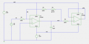
AC and Stability Analysis in NGSPICE

The above example shows an AC analysis test-bench GSCHEM. In this example the loop is broken by R3 whose value at dc is 1mO and is changed to 1TO for ac analysis. Doing this enables NGSPICE to converge on a sensible dc operating point for open loop analysis without any imperfections such as input offset forcing the output to one of the supply rails. [read more at http://education.ingenazure.com/]

Oct 13, 2014

Wearable Sensing and Computing

 Wearable Sensing and Computing 
 05.11.2014 - 06.11.2014
 EPFL Lausanne (CH)

COURSE OBJECTIVES
The course main objective is to inform and discuss in great details the latest advancements in low power sensing technology, energy harvesting and their heterogeneous integration for wearable smart system applications. Technological roadmaps of performance and future evolutions will be presented. The low power wireless communications are discussed from the point of view of existing standards and challenges for reducing the energy per communicated bit. Another objective is to detail some key future applications for wearable sensing and computing with main emphasis on: (1) medical Diagnostics, monitoring and prevention and (2) sports, fitness and activity monitoring applications. We analyze the benefits of autonomous smart system technology from many different points of view, including that of the individual, the physician, health care management, and society in general. We provide a rationale on the role of such technology as a component of the care cycle and the changes it can induce by reinforcing preventive strategies.

AGENDA on-line
Day 1 (09:00 – 17:00):

  • Introduction to wearable technology and energy efficient functions for autonomous smart systems
  • Energy efficient computing technologies and their importance for wearable applications:
  • Wearable low power sensor technology trends
  • Wearable low power communications technologies
  • Wearable energy harvesting technology trends

Day 2 (09:00 – 17:00):

  • Heterogeneous integration: solutions, roadmaps and trends for wearables
  • Context-driven embodiments by wearable systems and related applications and services
  • Market Trends for Mobile and Wearable Technology
  • Wearable autonomous smart systems: Applications to Medical Diagnostics, Monitoring and Prevention Paradigms using Feedback Loops
  • Wearable Technology – Sports, Fitness and Activity Monitoring Applications
Course registration on-line

Oct 7, 2014

[mos-ak] 7th International MOS-AK Workshop; December 12, 2014 at Berkeley

 7th International MOS-AK Workshop
 Berkeley Friday, Dec. 12, 2014 
 Announcement and Call for Papers 
 
 Together with the MOS-AK Workshop Scientific Program Coordinators Larry Nagel and Andrei Vladimirescu as well as Extended MOS-AK TPC Committee, we have pleasure to invite to the 7th consecutive International MOS-AK Workshop which will be held at Berkeley, California, USA, in the IEDM Conference and CMC Meeting timeframe. The event is organized with aims to strengthen a network and discussion forum among experts in the field, enhance open platform for information exchange related to compact/Spice modeling and Verilog-A standardization, bring people in the compact modeling field together, as well as obtain feedback from technology developers, circuit designers, and CAD/EDA tool vendors. 

Venue:
Room 540 in Cory Hall
EECS Department
University of California, Berkeley

Important Dates:
Call for Papers - September 2014
2nd Announcement - October 2014
Final Workshop Program - November. 2014
MOS-AK Workshop - Friday, Dec. 12, 2014
08:30 - 09:00 - On-site Registration 
09:00 - 11:00 - Morning MOS-AK Session
11:00 - 12:00 - CM Standardization Panel
12:00 - 13:00 - Lunch
13:00 - 16:00 - Afternoon MOS-AK Session 

Topics to be covered include the following:
  • Advances in semiconductor technologies and processing
  • Compact Modeling (CM) of the electron devices
  • Verilog-A language for CM standardization
  • New CM techniques and extraction software
  • Open Source TCAD/EDA modeling and simulation
  • CM of passive, active, sensors and actuators
  • Emerging Devices, CMOS and SOI-based memory cells
  • Microwave, RF device modeling, high voltage device modeling
  • Nanoscale CMOS devices and circuits
  • Technology R&D, DFY, DFT and IC Designs
  • Foundry/Fabless Interface Strategies
Abstract Submission:
Authors should submit an abstract using on-line MOS-AK submission form (any related inquiries can be sent to abstracts@mos-ak.org)
http://www.mos-ak.org/berkeley_2014/abstracts.php

On-line free workshop registration:
http://www.mos-ak.org/berkeley_2014/registration.php

Postworkshop publications:
Selected best MOS-AK technical presentation will be recommended for further publication in a special issue of the International Journal of High Speed Electronics and Systems

Extended MOS-AK/GSA Committee

WG06102014

--
You received this message because you are subscribed to the Google Groups "mos-ak" group.
To unsubscribe from this group and stop receiving emails from it, send an email to mos-ak+unsubscribe@googlegroups.com.
To post to this group, send email to mos-ak@googlegroups.com.
Visit this group at http://groups.google.com/group/mos-ak.
For more options, visit https://groups.google.com/d/optout.