Sep 14, 2022

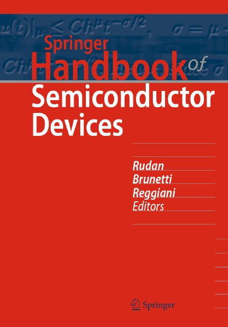
Handbook of Semiconductor Devices

Massimo Rudan, Rossella Brunetti, Susanna Reggiani (Eds.)
Springer Handbook of Semiconductor Devices
Series: Springer Handbooks
1st ed., 2022, ca. 1700 p., 1300 illus.

Order online at link.springer.com or customerservice@springernature.com
  • Covers physical backgrounds, fabrication, application and modeling
  • Describes in detail both conventional and innovative devices
  • An indispensable resource for practitioners, professionals and researchers


This Springer Handbook comprehensively covers the topic of semiconductor devices, embracing all aspects from theoretical background to fabrication, modeling, and applications.

Nearly 100 leading scientists from industry and academia were selected to write the handbook's chapters, which were conceived for professionals and practitioners, material scientists, physicists and electrical engineers working at universities, industrial R&D, and manufacturers.

Starting from the description of the relevant technological aspects and fabrication steps, the handbook proceeds with section fully devoted to the main conventional semiconductor devices like, e.g., bipolar transistors and MOS capacitors and transistors, used in the production of the standard integrated circuits, and the corresponding physical models. In the subsequent chapters, the scaling issues of the semiconductor-device technology are addressed, followed by the description of novel concept-based semiconductor devices. The last section illustrates the numerical simulation methods ranging from the fabrication processes to the device performances.

Each chapter is self-contained, and refers to related topics treated in other chapters when necessary, so that the reader interested in. specific subject can easily identify personal reading path through the vast contents of the handbook.

Technological aspects
CMOS Manufacturing processes. Semiconductor memory technologies. BCD process technologies. Measuring techniques for the semiconductor's parameters. Interconnect Processing: Integration, Dielectrics, Metals. Wet Chemical Processes for BEOL Technology. From FinFET to nanosheets and beyond. Advanced Lithography. Advanced technologies for future materials and devices

Basic devices and applications
MOS Capacitors, MOS Transistors and Charge-Transfer Devices. Electrostatic doping and devices. Planar MOSFETs and their application to IC design. Silicon power devices. Silicon Carbide Power Devices. GaN- based lateral and vertical devices. Bipolar transistors and silicon diodes. Memory Challenges. Silicon sensors. Solar Cells. X-ray detectors. Photodetectors based on Emerging Materials. Terahertz Electronic Devices. Semiconductor Lasers

New-generation devices and architectures
Heterojunction tunnel field-effect transistors. Carbon based field-effect transistors. Negative capacitors and applications. Flexible Electronics and Biomedical Sensors. Bio-Degradable Electronics. Resistive Switch- ing Memories. Phase-Change Memories. Spin-Based Devices for Digital Applications. Memristive/CMOS devices for neuromorphic applications. Nanoelectronic Systems for quantum computing

Modeling
Compact/SPICE Modeling. Process simulation. A digital twin for MEMS and NEMS. Macroscopic Transport Models for Classical Device Simulation. Grid generation and Algebraic solvers. Spherical Harmonics Expansion and Multi-Scale Modeling. Charge Transport Models for Amorphous Chalcogenides. Application of the k.p method to device simulation. Ab initio methods for electronic transport in semiconductors and nanostructures. Quantum Transport in the Phase Space, the Wigner Equation. The Non-Equilibrium Green Function (NEGF) Method. Tight-Binding Models, their Applications to Device Modeling and Deployment to. Global Community

[Steven Kosier] Google, National Institute of Standards and Technology (NIST), and SkyWater Technology Foundry bring wafer-level economies of scale to materials and device research through this CRADA!  #madeinamerica #freePDK #semi https://t.co/oI71mlHwfD


from Twitter https://twitter.com/wladek60

September 14, 2022 at 09:20AM
via IFTTT

Sep 4, 2022

[mos-ak] [online publications] Recent MOS-AK Workshops


The MOS-AK Association has organized two subsequent compact/SPICE modeling workshops, its selected MOS-AK presentations with assigned DOI Numbers are available online:
The MOS-AK Association plans to continue its standardization efforts by organizing future compact modeling meetings, workshops and panels around the globe thru the 2022 Year, including:
  • IRPhE'2022, Yerevan (AM) Sept. 27-30, 2022
  • MOS-AK Brazil Panel (BR), Oct. 2022
  • 15th US MOS-AK Workshop, Silicon Valley (US) Dec. 2022
    • in the timeframe of CMC and IEDM Meetings
W.Grabinski on the behalf of International MOS-AK Committee
WG040922


--
You received this message because you are subscribed to the Google Groups "mos-ak" group.
To unsubscribe from this group and stop receiving emails from it, send an email to mos-ak+unsubscribe@googlegroups.com.
To view this discussion on the web visit https://groups.google.com/d/msgid/mos-ak/CALp-Rj-F2meB1QwtSZT5wxez-_RR%3DOdj1ESpchGe8731f-CFAw%40mail.gmail.com.

[C4P] micro-nano 2022


Micro Nano 2022
9th International Conference on Micro-Nanoelectronics, Nanotechnology and MEMS
4-5 November 2022
Democritus University of Thrace, Vas. Sofias 12, 67132, Xanthi, Greece
https://2022.micro-nano.gr/

The annual conference is organized by the Micro&Nano Scientific Society of Greece and aims to connect people from academia, research and industry, to stimulate discussions on latest scientific achievements and further promote micro- and nanotechnology.

Important dates of the 9th International Micro-Nano Conference
  • Abstract submission deadline: 22 September 2022
  • Early bird registration: 7 October 2022
  • Late poster presentation: 16 October 2022
  • Conference: 4-5 November 2022
The conference committee encourages authors to submit papers on the thematic topics for oral or poster presentation.

Selected papers will be published in a special issue of Microelectronic Engineering, after peer review; see: Call for Papers and additional contact information: online form

TOPICS:
  • MATERIALS FOR ELECTRONICS, PHOTONICS & SENSORS
    • Semiconductors (Si-based, II-VI, III-V, SiC, Diamond)
    • Porous materials
    • Dielectrics
    • Organic materials
    • Self-assembling/self-organizing materials
    • Magnetic Materials
    • Metamaterials
    • Photonic Structures
  • MICRO AND NANO – FABRICATION
    • Front-end and back-end processes for IC fabrication
    • Patterning Technologies
    • Epitaxial growth
    • Self-assembly
    • Integration
    • Micromachining
    • Process Modeling and simulation
  • SENSORS AND ACTUATORS
    • Physical sensors
    • Chemical sensors
    • Bio-chemical sensors
    • Energy Harvesting devices
    • Microfluidics
    • MEMS
    • Detectors
  • ELECTRONIC, OPTOELECTRONIC AND PHOTONIC DEVICES
    • CMOS
    • Emerging non-CMOS
    • Devices based on 2-D materials
    • Microwave Devices
    • Thin Film Devices
    • Light Emitting and Organic electronic devices
    • Other Optoelectronic and Photonic Devices
  • MICRO AND NANO-TECHNOLOGY IN ENERGY
    • Energy storage (microbatteries, micro- and nano materials for electrodes, supecapacitors)
    • Energy harvesting (solar cells, electrostatic, piezoelectric)

Sep 3, 2022

Exploded view of first ASIC, inside the TinyTapeout project

Exploded view of my first ASIC, inside the TinyTapeout project 


from Twitter https://twitter.com/wladek60

September 03, 2022 at 09:15PM
via IFTTT