Aug 31, 2020

Opinion Can Israel lead the #opensource code revolution? The Israeli tech scene is based on partnerships, innovation and independent thinking which are all vital in open-source code https://t.co/GdyYArG2sa https://t.co/yG6MPmp7bG


from Twitter https://twitter.com/wladek60

August 31, 2020 at 10:31AM
via IFTTT

Aug 28, 2020

TSMC: All the Processes, All the Fabs

TSMC Technology Symposium: All the Processes, All the Fabs
by Paul McLellan at breakfast-bytes
27 Aug 2020

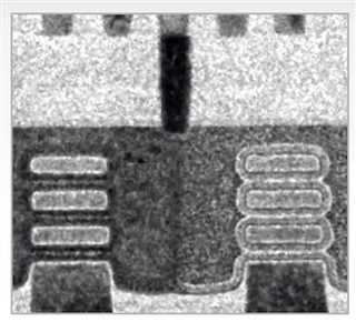
TSMC has new transistor structure (nanosheet) and new materials such as high mobility channel, 2D, carbon nanotube (CNT). TSMC has already demonstrated at 32Mb nanosheet SRAM fully-functional at 0.46V. It has also identified promising 2D materials such as MoS2 (molybdenum disulfide). At IEDM last year, they disclosed the first BEOL CNT power-gating device integrated with silicon-based CMOS.
Scaling continues with EUV advances with the current generation of scanners. They are also working with ASML (the only supplier of EUV equipment) on High-NA EUV [read more...]


Aug 27, 2020

Chip in the Fields: SBCCI and SBMicro Conferences

Chip in the Fields
C̶a̶m̶p̶i̶n̶a̶s̶,̶ ̶S̶P̶,̶ ̶B̶r̶a̶z̶i̶l̶ ̶ 
Virtual
August 24 to 28, 2020

Due to the COVID-19 pandemic the Chip in the Fields is changed to a virtual event. In 2021 we plan to have again the normal live Chip in the Fields events to be held in Hotel Premium, Campinas, SP, Brazil

The conferences SBCCI and SBMicro started in the early 80’s and since the year 2000 they joined forces, organizing them at the same venue and under a unified fantasy name “Chip in Somewhere”. The somewhere could be the name of the city or a fantasy name related to the region. It started with the name of “Chip in the Jungle”, because it was held in Manaus, the heart of the Amazon forest. 

Along these 21 years of Chip in, gradually other conferences joined the common venue and organization. Nowadays, we are composed of five sister conferences: SBCCI, SBMicro, WCAS, INSCIT and Sforum, as described in the respective call for papers. Due to the COVID-19 pandemic the Chip in the Fields is changed to a virtual event. Detalhes of the program and access link will be made available in the near future. Please follow the conference website for future up-dates.

Keynote Speakers

Kenneth K. O

Texas Analog Center of Excellence and Dept. of ECE,
The University of Texas at Dallas, Richardson, TX

Rajiv V. JoshiT. J. Watson research center, IBM                                         


Sponsored by:

Co-sponsored by:

Organized by:

Supported by:

Silicon Sponsors:

Platinum Sponsors:

Silver Sponsors:


Events:

Aug 26, 2020

[paper] SiC MOSFET Corner and Statistical SPICE Model Generation

SiC MOSFET Corner and Statistical SPICE Model Generation
Canzhong He, James Victory* , Yunpeng Xiao**, Herbert De Vleeschouwer+
Elvis Zheng++, ZhiPing Hu++ 
 ISPSD, September 13-18, 2020, Vienna, Austria
DOI: 10.1109/ISPSD46842.2020.9170091

   Power Design Enablement, ON Semiconductor, Mountain Top, Pennsylvania/USA
 *Power Design Enablement, ON Semiconductor, Aschheim, Germany
**Power Design Enablement, ON Semiconductor, Shanghai, China 
 +Wide Bandgap Technology Development, ON Semiconductor, Oudenaarde, Belgium 
++Product & Test Development Center, ON Semiconductor, Suzhou, China

Abstract: This paper presents a novel approach to generate corner and statistical SPICE models for SiC MOSFETs. The technique is derived from the mature IC industry standard approach known as Backward Propagation of Variance. Physically based, scalable SiC MOSFET SPICE models are required to simulate the correlations between electrical specifications and process variations. The methodologies presented are applicable to other power discrete devices such as super-junction MOSFETs, IGBTs, and GaN HEMTs.

Fig.: SiC MOSFET (a) Cross Section, (b) Subcircuit SPICE Model


Aug 25, 2020

[paper] Native High-k Oxides for 2D Transistors

Yury Yu. Illarionov1,2, Theresia Knobloch1 and Tibor Grasser1
Native high-k oxides for 2D transistors
Nature Electronics vol. 3, pp 442–443 (2020)
Published online: 05 August 2020
DOI: 10.1038/s41928-020-0464-2

1Institute for Microelectronics, TU Wien, Vienna, Austria
2Ioffe Physical-Technical Institute, St Petersburg, Russia

Abstract: The two-dimensional semiconductor Bi2O2Se can be oxidized to create an atomically thin layer of Bi2SeO5 that can be used as the insulator in scaled field-effect transistors.

Fig.: Development of FETs with Bi2O2Se channels and native Bi2SeO5 insulators. a.) Step-by-step oxidation of multilayer Bi2O2Se towards Bi2SeO5 and the crystal structure of the two materials. b.) Cross-sectional scanning transmission electron microscopy image confirming the atomically sharp interface. c.) Schematic of the top-gated devices fabricated with a native gate oxide. d.) Gate transfer characteristics of the devices with a 4.6-nm-thick Bi2SeO5 layer (EOT below 1 nm)