May 18, 2020

[paper] Novel Design and Optimization and the gm/ID Ratio

A Novel Design and Optimization Approach for Low Noise Amplifiers (LNA) Based on MOST Scattering Parameters and the gm/ID Ratio
1Facultad de Ingeniería, Universidad Católica de Córdoba, Córdoba 5017 (AN)
2Service d’Électronique et Microélectronique, Université de Mons (UMONS), 7000 Mons (BE)
3Departamento de Electrónica, Instituto de Astrofísica de Canarias (IAC), 38200 La Laguna (SP)
* Author to whom correspondence should be addressed.
Electronics 2020, 9(5), 785; https://doi.org/10.3390/electronics9050785
Received: 31 March 2020 / Revised: 30 April 2020 
Accepted: 9 May 2020 / Published: 11 May 2020

AbstractThis work presents a new design methodology for radio frequency (RF) integrated circuits based on a unified analysis of the scattering parameters of the circuit and the gm/ID ratio of the involved transistors. Since the scattering parameters of the circuits are parameterized by means of the physical characteristics of transistors, designers can optimize transistor size and biasing to comply with the circuit specifications given in terms of S-parameters. A complete design of a cascode low noise amplifier (LNA) in 65nm CMOS technology is taken as a case study in order to validate the approach. In addition, this methodology permits the identification of the best trade-off between the minimum noise figure and the maximum gain for the LNA in a very simple way.
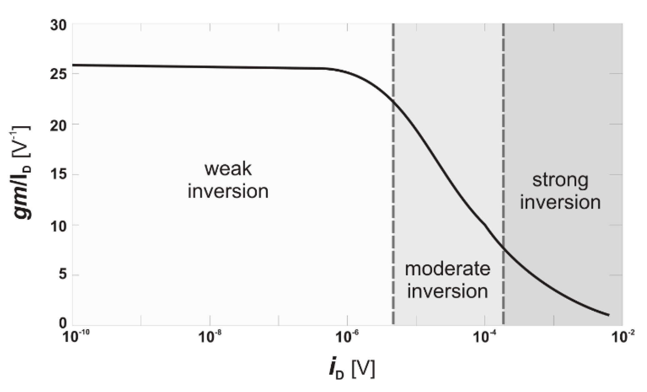
Figure: gm/ID versus iD

Acknowledgement - This research was funded by Universidad Católica de Córdoba (Argentina), the Walloon Region DGO6 BEWARE Fellowships Academia Programme (1410164-POHAR, cofunded by the European Marie Curie Actions), the Belgian FNRS (Fond National pour la Recherche Scientifique) and the Argentinean MINCyT (Ministerio de Ciencia y Tecnología).

May 15, 2020

[paper] Electrical characterization of advanced MOSFETs

Valeriya Kilchytska, Sergej Makovejev, Babak Kazemi Esfeh, Lucas Nyssens, Arka Halder,
Jean-Pierre Raskin and Denis Flandre
Electrical characterization of advanced MOSFETs towards analog and RF applications
IEEE LAEDC, San Jose, Costa Rica, 2020, 
doi: 10.1109/LAEDC49063.2020.9073536

Abstract - This invited paper reviews main approaches in the electrical characterization of advanced MOSFETs towards their target analog and RF applications. Advantages and necessity of those techniques will be demonstrated on different study cases of various advanced MOSFETs, such as FDSOI, FinFET, NW in a wide temperature range, based on our original research over the last years. 

URL: https://ieeexplore.ieee.org/stamp/stamp.jsp?tp=&arnumber=9073536&isnumber=9072949

Acknowledgements - This work was partially funded by Eniac “Places2Be”, Ecsel “Waytogofast”, FNRS - FRFC “Towards Highly-efficient 10 nm MOSFETs”, FP7 “Nanosil” and “Nanofunction” projects. The authors thank our colleagues from CEA-Leti, ST and Imec, and particularly, F. Andrieu, O. Faynot, T. Poiroux, S. Barraud, M. Haond, N. Planes, N. Collaert, C. Claeys, M. Jurczak, B. Parvais, R. Rooyackers, for providing UTBB FD SOI, NW and FinFET devices and valuable discussions.