May 23, 2020

[PhD] Printed Inorganic Materials Electronics

Circuit Design and Compact Modeling in Printed Electronics Based on Inorganic Materials
PhD Dissertation
Gabriel Cadilha Marques
Veröffentlicht am 30.04.2020
DOI: 10.5445/IR/1000118801

Abstract - The goal of this thesis is therefore to develop an inorganic printed electronics technology with corresponding modeling methodologies to capture device behavior for industry standard circuit simulators as well as circuit designs as building blocks for future applications. To reduce the high supply voltage requirements (~5V) in PE, alternative gating approaches for FETs are considered. One approach is to replace the dielectric with an electrolyte. Due to the formation of a Helmholtz double layer (HDL), a FET with a high gate-capacitance (~5 μFcm-2) is expected, reducing the voltage requirements to ~1V. By combining the indium oxide channel with the electrolyte-gating approach, high performance devices with low voltage requirements are available in PE.


May 19, 2020

[paper] Polymer Electrodes in Clinical EEG and MEG

Laura M. Ferrari, Usein Ismailov, Jean-Michel Badier, Francesco Greco and Esma Ismailova 
Conducting polymer tattoo electrodes in clinical electro- and magneto-encephalography
npj Flex Electron 4, 4 (2020)
Received: 17 October 2019; Accepted: 20 February 2020;
DOI: 10.1038/s41528-020-0067-z

Abstract - Temporary tattoo electrodes are the most recent development in the field of cutaneous sensors. They have successfully demonstrated their performances in the monitoring of various electrophysiological signals on the skin. These epidermal electronic devices offer a conformal and imperceptible contact with the wearer while enabling good quality recordings over time. Evaluations of brain activity in clinical practice face multiple limitations, where such electrodes can provide realistic technological solutions and increase diagnostics efficiency. Here we present the performance of inkjet-printed conducting polymer tattoo electrodes in clinical electroencephalography and their compatibility with magnetoencephalography. The working mechanism of these dry sensors is investigated through the modeling of the skin/electrode impedance for better understanding of the biosignals transduction at this interface. Furthermore, a custom-made skin phantom platform demonstrates the feasibility of high-density recordings, which are essential in localizing neuropathological activities. These evaluations provide valuable input for the successful application of these ultrathin electronic tattoos sensors in multimodal brain monitoring and diagnosis.

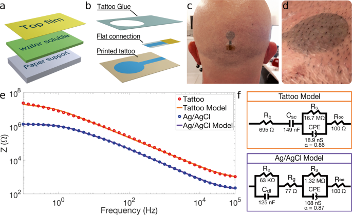
figure1
Fig: Temporary tattoo electrodes (TTEs) for EEG: a The layered structure of the temporary tattoo paper permits the release of the top film on which electrodes are fabricated. b Expanded view of an all-polymer printed TTE. c A TTE released on the scalp, in Oz position. d Close-in view of a TTE released on the scalp after 12 h from application. e Impedance recordings on the forearm using TTE and Ag/AgCl electrodes. 
Experiments involving human participants -Two able-bodied participants (one male and one female aged 33.5 ± 3.5 years old) free of any motor and neural disorders gave their informed consent and participated in this study. One participant performed the impedance recordings with the three diverse TTEs sets while another participant volunteered in the EEG/MEG evaluations with TTEs and Ag/AgCl electrodes. All experiments are performed following Timone hospital’s regulations regarding personal data protection. The experiment was conducted under conditions provided by French regulations.

Data Availability - The experimental data referenced in this text is available from the authors upon reasonable request.

#EU Parliament Strongly Recommends Developing and Using #opensource Software https://t.co/6HxdUaUHQK https://t.co/7czSKFmwh7


from Twitter https://twitter.com/wladek60

May 19, 2020 at 10:00AM
via IFTTT

May 18, 2020

[paper] Novel Design and Optimization and the gm/ID Ratio

A Novel Design and Optimization Approach for Low Noise Amplifiers (LNA) Based on MOST Scattering Parameters and the gm/ID Ratio
1Facultad de Ingeniería, Universidad Católica de Córdoba, Córdoba 5017 (AN)
2Service d’Électronique et Microélectronique, Université de Mons (UMONS), 7000 Mons (BE)
3Departamento de Electrónica, Instituto de Astrofísica de Canarias (IAC), 38200 La Laguna (SP)
* Author to whom correspondence should be addressed.
Electronics 2020, 9(5), 785; https://doi.org/10.3390/electronics9050785
Received: 31 March 2020 / Revised: 30 April 2020 
Accepted: 9 May 2020 / Published: 11 May 2020

AbstractThis work presents a new design methodology for radio frequency (RF) integrated circuits based on a unified analysis of the scattering parameters of the circuit and the gm/ID ratio of the involved transistors. Since the scattering parameters of the circuits are parameterized by means of the physical characteristics of transistors, designers can optimize transistor size and biasing to comply with the circuit specifications given in terms of S-parameters. A complete design of a cascode low noise amplifier (LNA) in 65nm CMOS technology is taken as a case study in order to validate the approach. In addition, this methodology permits the identification of the best trade-off between the minimum noise figure and the maximum gain for the LNA in a very simple way.
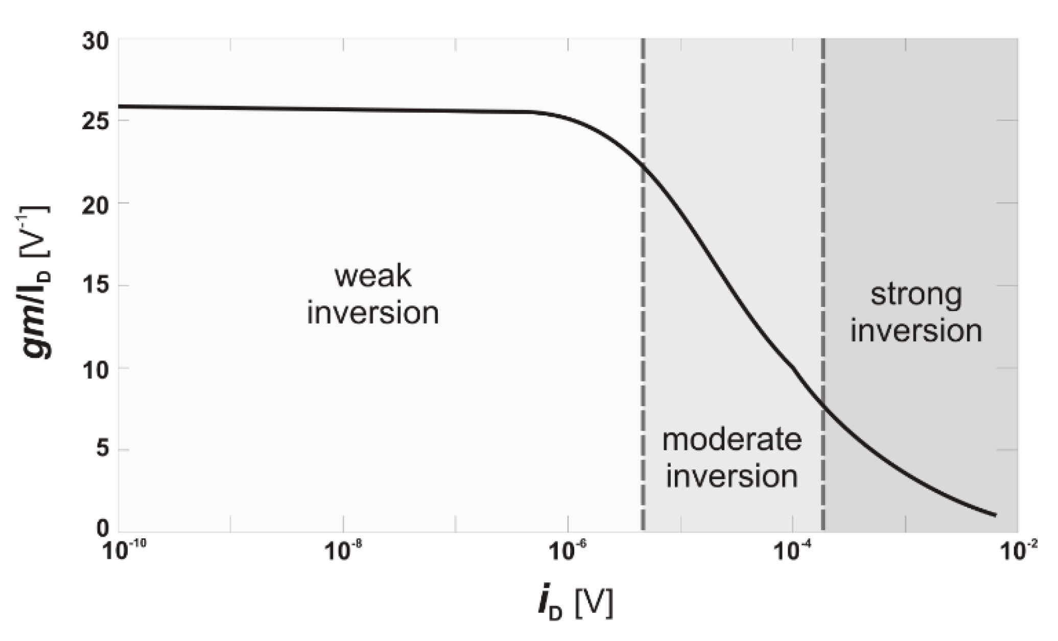
Figure: gm/ID versus iD

Acknowledgement - This research was funded by Universidad Católica de Córdoba (Argentina), the Walloon Region DGO6 BEWARE Fellowships Academia Programme (1410164-POHAR, cofunded by the European Marie Curie Actions), the Belgian FNRS (Fond National pour la Recherche Scientifique) and the Argentinean MINCyT (Ministerio de Ciencia y Tecnología).

May 15, 2020

[paper] Electrical characterization of advanced MOSFETs

Valeriya Kilchytska, Sergej Makovejev, Babak Kazemi Esfeh, Lucas Nyssens, Arka Halder,
Jean-Pierre Raskin and Denis Flandre
Electrical characterization of advanced MOSFETs towards analog and RF applications
IEEE LAEDC, San Jose, Costa Rica, 2020, 
doi: 10.1109/LAEDC49063.2020.9073536

Abstract - This invited paper reviews main approaches in the electrical characterization of advanced MOSFETs towards their target analog and RF applications. Advantages and necessity of those techniques will be demonstrated on different study cases of various advanced MOSFETs, such as FDSOI, FinFET, NW in a wide temperature range, based on our original research over the last years. 

URL: https://ieeexplore.ieee.org/stamp/stamp.jsp?tp=&arnumber=9073536&isnumber=9072949

Acknowledgements - This work was partially funded by Eniac “Places2Be”, Ecsel “Waytogofast”, FNRS - FRFC “Towards Highly-efficient 10 nm MOSFETs”, FP7 “Nanosil” and “Nanofunction” projects. The authors thank our colleagues from CEA-Leti, ST and Imec, and particularly, F. Andrieu, O. Faynot, T. Poiroux, S. Barraud, M. Haond, N. Planes, N. Collaert, C. Claeys, M. Jurczak, B. Parvais, R. Rooyackers, for providing UTBB FD SOI, NW and FinFET devices and valuable discussions.