Showing posts with label TID. Show all posts

Apr 11, 2022

[paper] Noise Degradation and Recovery in Gamma-irradiated SOI nMOSFET

S.Amorab, V.Kilchytskaa, F.Tounsia, N.Andréa, M.Machhoutb, L.A.Francisa, D.Flandrea
Characteristics of noise degradation and recovery in gamma-irradiated SOI nMOSFET
with in-situ thermal annealing
Solid-State Electronics; 108300; online 7 April 2022, 
DOI: 10.1016/j.sse.2022.108300
   
a SMALL, ICTEAM Institute, Université catholique de Louvain (B)
b Faculté des Sciences de Université de Monastir (TN)


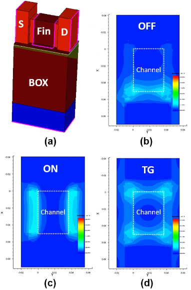
Abstract: This paper demonstrates a procedure for complete in-situ recovery of on-membrane CMOS devices from total ionizing dose (TID) defects induced by gamma radiation. Several annealing steps were applied using an integrated micro-heater with a maximum temperature of 365°C. The electrical characteristics of the on-membrane nMOSFET are recorded prior and during irradiation (up to 348 krad (Si)), as well as after each step of the in-situ thermal annealing. High-resolution current sampling measurements reveal the presence of oxide defects after irradiation, with a clear dominant single-trap signature in the random telegraph noise (RTN) traces. Drain current over time measurements are used for the trap identification and further for the defects' parameters extraction. The power spectral density (PSD) curves confirm a clear dominance of the RTN behavior in the low-frequency noise. A radiation-induced oxide trap is detected at 5.4 nm from the Si-SiO2 interface, with an energy of 0.086 eV from the Fermi level in the bandgap. After annealing, the RTN behavior vanishes with a further important reduction of flicker noise. Low-frequency noise measurements of the transistor confirmed the neutralization of oxide defects after annealing. The electro-thermal annealing of the nMOSFET allows a total recovery of its original characteristics after being severely degraded by radiation-induced defects.

Fig: Device under test : (a) cross-section schematic, (b) microscopic front view
showing the membrane and other embedded elements


Jun 2, 2020

[paper] TID Effects in SOI FinFETs

Bias and geometry dependence of total-ionizing-dose effects in SOI FinFETs
Zhexuan Ren1, Xia An1, Gensong Li1, Runsheng Wang1, Nuo Xu2, Xing Zhang1 and Ru Huang1
1Institute of Microelectronics, Peking University, Beijing 100871, CN
2Department of Electrical Engineering and Computer Sciences, UCB, CA 94720, USA
Semiconductor Science and Technology, Volume 35, Number 7

Abstract: In this paper, a systematic research on the total-ionizing-dose (TID) effects of NMOS and PMOS silicon-on-insulator (SOI) FinFETs is performed experimentally. The bias and geometry dependence of TID effects are analysed. The experimental results show that the threshold voltage (Vth) shift occurs in SOI FinFETs after x-ray irradiation. After 1 Mrad (Si) irradiation, the maximum Vth shift is about 40 mV. The 'worst case' irradiation bias conditions for NMOS and PMOS are TG and ON states, respectively, which induces the largest Vth shift after irradiation. The 3D TCAD simulation is carried out to further analyse the bias dependence results. Simulation results highlight the difference in electric field distribution in the buried oxide under different bias configurations, which leads to different distribution of irradiation-induced trapped charges. Finally, clear geometry dependence is observed in the TID experiment. Both NMOS and PMOS devices with larger fin width and/or smaller gate length are more sensitive to TID irradiation. The results deepen the understanding of the TID effect of SOI FinFETs and provide important technical support for the radiation-hardened research of FinFET technology.

Figure: (a) SOI NMOS FinFET in 3D TCAD software with Z-cut in BOX layer. Simulated electric field distribution in Z-cut plane for OFF (b), ON (c) and TG (d) bias conditions. The white dashed box in figure (b), (c), (d) indicates the relative position of the channel region.

Acknowledgments: This work was supported in part by the National Natural Science Foundation of China (No.61421005, 61434007) and 111 Project (B18001). The authors would like to thank the staff of the Xinjiang Technical Institute of Physics and Chemistry (XTIPC), Chinese Academy of Sciences (CAS) for their assistance in the TID irradiation experiment.