Jun 8, 2020

[paper] NESS

Nano-electronic Simulation Software (NESS): 
a flexible nano-device simulation platform
Salim Berrada, Hamilton Carrillo-Nunez, Jaehyun Lee, Cristina Medina-Bailon, Tapas Dutta, Oves Badami, Fikru Adamu-Lema, Vasanthan Thirunavukkarasu, Vihar Georgiev and Asen Asenov 
Journal of Computational Electronics (2020)
DOI: 10.1007/s10825-020-01519-0

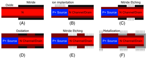
Abstract: The aim of this paper is to present a flexible and open-source multi-scale simulation software which has been developed by the Device Modelling Group at the University of Glasgow to study the charge transport in contemporary ultra-scaled Nano-CMOS devices. The name of this new simulation environment is Nano-electronic Simulation Software (NESS). Overall NESS is designed to be flexible, easy to use and extendable. Its main two modules are the structure generator and the numerical solvers module. The structure generator creates the geometry of the devices, defines the materials in each region of the simulation domain and includes eventually sources of statistical variability. The charge transport models and corresponding equations are implemented within the numerical solvers module and solved self-consistently with Poisson equation. Currently, NESS contains a drift–diffusion, Kubo–Greenwood, and non-equilibrium Green’s function (NEGF) solvers. The NEGF solver is the most important transport solver in the current version of NESS. Therefore, this paper is primarily focused on the description of the NEGF methodology and theory. It also provides comparison with the rest of the transport solvers implemented in NESS. The NEGF module in NESS can solve transport problems in the ballistic limit or including electron–phonon scattering. It also contains the Flietner model to compute the band-to-band tunneling current in heterostructures with a direct band gap. Both the structure generator and solvers are linked in NESS to supporting modules such as effective mass extractor and materials database. Simulation results are outputted in text or vtk format in order to be easily visualized and analyzed using 2D and 3D plots. The ultimate goal is for NESS to become open-source, flexible and easy to use TCAD simulation environment which can be used by researchers in both academia and industry and will facilitate collaborative software development.
FIG: Flowchart of NESS detailing its modular structure

NESS will be released in the summer of 2020 as an open-source software which makes it very interesting for both academia and industry in helping to address the challenges subsequent to the further down-scaling of CMOS components.

Acknowledgements: This work was supported by the European Union’s Horizon 2020 research and innovation programme under Grant Agreement No. 688101 SUPERAID7. Also, this project has received funding from EPSRC UKRI under Grant Agreements No. EP/S001131/1 (QSEE) and No. EP/P009972/1 (QUANTDEVMOD).

Semi-talk: Low Cost Photonics | Dr. Naresh Chand, Life Fellow of IEEE, Associate Vice President, Chapter Relations of the IEEE Photonics Society https://t.co/mQkIAGoI51 #paper https://t.co/zmPh8QDa3F


from Twitter https://twitter.com/wladek60

June 08, 2020 at 09:52AM
via IFTTT

The Simplest #Microwave #Receiver https://t.co/atbhia4ZZy #paper https://t.co/WZDsDvXeoD


from Twitter https://twitter.com/wladek60

June 08, 2020 at 09:16AM
via IFTTT

Jun 5, 2020

[paper] Electrostatically doped drain engineered DG‐TFET

Shaikh, MRU, Loan, SA, Alshahrani, A.
Electrostatically doped drain engineered DG‐TFET:
Proposal and Analysis

IJNM 2020;e2769
DOI: 10.1002/jnm.2769

Abstract: In this paper, a drain‐engineered double‐gate Tunnel‐FET (DE‐DG‐TFET) to enhance the electrical characteristics and analog parameters of a conventional DG‐TFET is proposed and examined through calibrated TCAD simulations. Unlike DG‐TFET, a constant n‐type doping, Ncd, (5E17 cm−3 − 2E18 cm−3), in the channel/drain regions of DE‐DG‐TFET is used, resulting in a p+‐n‐n structure instead of conventional p+‐i‐n structure. Further, p+‐n‐n is modified to p+‐n‐n+ using electrostatic doping (ED) method on the drain side with Hafnium (ϕm = 3.9 eV) as a lateral (top and bottom) and side metal electrode. A high n+‐drain doping ensures the drain contact remains ohmic. Higher electric field at p+‐n source‐channel junction enhances the ON‐state BTBT current. While the absence of metallurgical junction provides large tunneling width across the channel/drain junction, resulting in suppression of ambipolar current (IAMB). At Ncd doping of 1E18 cm−3, DE‐DG‐TFET demonstrates ~7 times increase in ION while IAMB is suppressed by ~5 orders of magnitude. In addition to this, the proposed device improves analog/RF figures of merit, 45% in voltage gain and ~5 times in peak fT.

FIG: Key steps for fabrication of the proposed DEDG-TFET

Acknowledgement: This work was supported by Ministry of Electronics & Information Technology (MeitY), Government of India through Visvesvaraya PhD Scheme.

Reading about #OpenSource in French https://t.co/A5lXEvoSOL https://t.co/OjByvKO4la


from Twitter https://twitter.com/wladek60

June 05, 2020 at 10:55AM
via IFTTT

Jun 4, 2020

[paper] Large-signal behavioral model for RF power transistors

Cai J, King J, Liu J, Wang J, Sun L.
Large-signal behavioral model for radio frequency power transistors 
based on modified canonical sectionwise piecewise-linear functions
IJNM 2020;e2767
DOI: 10.1002/jnm.2767

Abstract: A novel, large-signal behavioral modeling methodology for radio frequency power transistors, based on the modified canonical sectionwise piecewiselinear (CSWPL) functions, is presented in this article. The basic theory of the proposed model is provided. Compared with the existing standard CSWPL model, the proposed model provides superior prediction capabilities for a reasonable increase in model complexity. Model verification is performed through comparisons with simulated and experimental data of a 10 W GaN HEMT device at mild and severe mismatch conditions, across a wide range of input power levels. The models can predict, more accurately, both the fundamental and the second harmonic scattered waves compared with the standard CSWPL model.
Fig: Comparison between circuit, CSWPL model, and proposed modified CSWPL model, when the available input power is 5dBm, the number of partitions K=J=3, and the number of Fourier terms L=3

Correspondence: Jialin Cai, The Key Laboratory of RF Circuit and System, Ministry of Education, Hangzhou Dianzi University, Hangzhou, CN


[paper] Unified Analytical Transregional MOSFET Model

Kalra, S, Bhattacharyya, AB. 
A Unified Analytical Transregional MOSFET Model for Nanoscale CMOS Digital Technologies
Int J Numer Model. 2020; 33:e2700
https://doi.org/10.1002/jnm.2700

Abstract: For IC designers, power has always been the main design constraint. Near threshold (moderate inversion) computing is a promising technique to manage power and energy requirements. A modeling framework specific to moderate inversion is developed in literature known as Transregional Mosfet Model (TRM). This paper presents an extension of TRM model by considering the lateral and vertical field dependent mobility of carriers that make it suitable for circuit design at supply voltages not restricted to near threshold voltage. The model proposed is the unified model applicable in all operating regions (weak, moderate, and strong) and all saturation levels from a long channel with negligible effect of velocity saturation to a short channel having extreme velocity saturation. Further, it has been shown that the proposed drain current model can be reduced to unified interpolated expression of EKV model for long channel MOSFET.

FIG: Comparison of (A) proposed model, (B) weak inversion approximation, (C) strong inversion approximation, with transregional MOSFET model (TRM) and BSIM4 at 22nm technology node.