
Shaikh, MRU, Loan, SA, Alshahrani, A.
Electrostatically doped drain engineered DG‐TFET:
Proposal and Analysis
IJNM 2020;e2769
DOI: 10.1002/jnm.2769
Electrostatically doped drain engineered DG‐TFET:
Proposal and Analysis
IJNM 2020;e2769
DOI: 10.1002/jnm.2769
Abstract:
In this paper, a drain‐engineered double‐gate Tunnel‐FET (DE‐DG‐TFET) to enhance the electrical characteristics and analog parameters of a conventional DG‐TFET is proposed and examined through calibrated TCAD simulations. Unlike DG‐TFET, a constant n‐type doping, Ncd, (5E17 cm−3 − 2E18 cm−3), in the channel/drain regions of DE‐DG‐TFET is used, resulting in a p+‐n‐n structure instead of conventional p+‐i‐n structure. Further, p+‐n‐n is modified to p+‐n‐n+ using electrostatic doping (ED) method on the drain side with Hafnium (ϕm = 3.9 eV) as a lateral (top and bottom) and side metal electrode. A high n+‐drain doping ensures the drain contact remains ohmic. Higher electric field at p+‐n source‐channel junction enhances the ON‐state BTBT current. While the absence of metallurgical junction provides large tunneling width across the channel/drain junction, resulting in suppression of ambipolar current (IAMB). At Ncd doping of 1E18 cm−3, DE‐DG‐TFET demonstrates ~7 times increase in ION while IAMB is suppressed by ~5 orders of magnitude. In addition to this, the proposed device improves analog/RF figures of merit, 45% in voltage gain and ~5 times in peak fT.
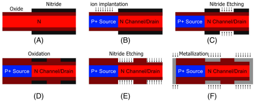
FIG: Key steps for fabrication of the proposed DEDG-TFET
Acknowledgement: This work was supported by Ministry of Electronics & Information Technology (MeitY), Government of India through Visvesvaraya PhD Scheme.