Arbeitskreis Modellierung von Systemen und Parameterextraktion
Modeling of Systems and Parameter Extraction Working Group
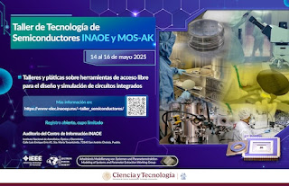
MOS-AK INAOE Workshop
Puebla (MX), May 14-16, 2025
The semiconductor industry is crucial for Mexico's development, and it is the key for the future growth of the country economics. Producing advanced integrated circuits involves many steps, beginning with the idea for the circuits, technology, IC design and its simulation, layout generation, manufacturing and functional tests, among them. All of these stages require dedicated, specialized software programs, generally very expensive, which makes them onerous for the majority of academic institutions in the country. Recently, however, there has been an important effort in developing free open source tools for this purpose, and thus accessible to any educational institutions. These include open source tools spanning from the design to the fabrication of the circuits. In these initial stages, having these tools available aims at fostering research and education in the field of prototyping IC design, without considering manufacturing in large quantities.
The mail goal of MOS-AK INAOE workshop is to expound on the available free open source tools for each IC development step in the design, simulation and manufacturing of integrated circuits, as well as presenting the options for the fabrication of ICs.
It is very important to train people, build the semi workforce with the basic knowledge needed to grow the semiconductor industry in Mexico. Professionals, including international researchers and experts from INAOE and other institutions, will give talks and courses to explain the tools, their potential uses, showing the engineering requirements and IC design applications.
Space is limited, so we invite you to
register at the following link:
-- R.Murphy and W.Grabinski
-- on the behalf of the MOS-AK INAOE Organizing Committee
Enabling Compact Modeling R&D Exchange
WG230425
--
You received this message because you are subscribed to the Google Groups "mos-ak" group.
To unsubscribe from this group and stop receiving emails from it, send an email to
mos-ak+unsubscribe@googlegroups.com.
To view this discussion visit
https://groups.google.com/d/msgid/mos-ak/CALp-Rj-udrUUkRt0cLK_pd1FhrA8Hb2UsuE8y3qpnjTySQgJzg%40mail.gmail.com.