Nov 16, 2020

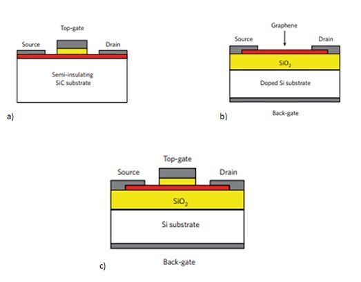
What Is a Graphene Field Effect Transistor (#GFET)?


from Twitter https://twitter.com/wladek60

November 16, 2020 at 10:21AM
via IFTTT

Nov 13, 2020

Digi-Key releases 1.5 million SnapEDA #CAD #models https://t.co/IzCT3WnWTC #semi https://t.co/BBXV146WQ7


from Twitter https://twitter.com/wladek60

November 13, 2020 at 07:47PM
via IFTTT

RT @gvanrossum: I decided that retirement was boring and have joined the Developer Division at Microsoft. To do what? Too many options to say! But it’ll make using Python better for sure (and not just on Windows :-). There’s lots of open source here. Watch this space. . #semi https://t.co/kJI0LT4jUA


from Twitter https://twitter.com/wladek60

November 13, 2020 at 07:35PM
via IFTTT

Nov 12, 2020

Fwd: Elena Gnani DL - Tunnel FETs: Device Physics and Realizations

To view complete details for this event, click here to view the announcement

Elena Gnani DL - Tunnel FETs: Device Physics and Realizations


The EDS Germany Chapter and NanoP proudly presents Elena Gnani from University of Bologna, Bologna, Italy for a Distinguished Lecture on "Tunnel FETs: Device Physics and Realizations". The lecture will be held on 18th January 2021 at 3pm Berlin time.

Date and Time

Location

The Distiguished Lecture will be held via Zoom. Login information provided before the event and requires registration.

Hosts

Registration

  • Starts 12 November 2020 04:30 PM
  • Ends 16 January 2021 05:00 PM
  • All times are Europe/Berlin
  • No Admission Charge

Nov 10, 2020

[mos-ak] [2nd Announcement and C4P] 13th Virtual MOS-AK Workshop, Silicon Valley, Dec. 10-11 2020


Together with  local organization team, International MOS-AK Board of R&D Advisers as well as all the Extended MOS-AK TPC Committee, we have the pleasure to invite to consecutive, 13th International MOS-AK Workshop which will be organized as the virtual/online event on Dec. 10-11, 2020 (preceding the IEDM and Q4 CMC Meetings)

Planned virtual 13th International MOS-AK Workshop aims to strengthen a network and discussion forum among experts in the field, enhance open platform for information exchange related to compact/SPICE modeling and Verilog-A standardization, bring academic and industrial experts in the compact modeling field together, as well as obtain feedback from technology developers, circuit designers, and CAD/EDA tool developers and vendors. 

Venue: Virtual/Online

Online Workshop Registration to be open 
(any related enquiries can be sent to registration@mos-ak.org)

Topics to be covered include the following among other related to the compact/SPICE modeling and its Verilog-A standardization:
  • Compact Modeling (CM) of the electron devices
  • Advances in semiconductor technologies and processing
  • Verilog-A language for CM standardization
  • New CM techniques and extraction software
  • Open Source (FOSS) TCAD/EDA modeling and simulation
  • CM of passive, active, sensors and actuators
  • Emerging Devices, TFT, CMOS and SOI-based memory cells
  • Microwave, RF device modeling, high voltage device modeling
  • Nanoscale CMOS, BiCMOS, SiGe, GaN, InP devices and circuits
  • Technology R&D, DFY, DFT and reliability/ageing IC designs
  • Foundry/Fabless Interface Strategies
Important Dates: 
  • 2nd Announcement: Nov. 2020
  • Final Workshop Program: Dec. 2020
  • Virtual MOS-AK Workshop: Dec. 10-11, 2020
Online Abstract Submission to be open 
(any related enquiries can be sent to abstbstracts@mos-ak.org)

WG10112020

--
You received this message because you are subscribed to the Google Groups "mos-ak" group.
To unsubscribe from this group and stop receiving emails from it, send an email to mos-ak+unsubscribe@googlegroups.com.
To view this discussion on the web visit https://groups.google.com/d/msgid/mos-ak/891cd84d-b714-44b6-85af-4e361a257515n%40googlegroups.com.