Jun 5, 2020

[paper] Electrostatically doped drain engineered DG‐TFET

Shaikh, MRU, Loan, SA, Alshahrani, A.
Electrostatically doped drain engineered DG‐TFET:
Proposal and Analysis

IJNM 2020;e2769
DOI: 10.1002/jnm.2769

Abstract: In this paper, a drain‐engineered double‐gate Tunnel‐FET (DE‐DG‐TFET) to enhance the electrical characteristics and analog parameters of a conventional DG‐TFET is proposed and examined through calibrated TCAD simulations. Unlike DG‐TFET, a constant n‐type doping, Ncd, (5E17 cm−3 − 2E18 cm−3), in the channel/drain regions of DE‐DG‐TFET is used, resulting in a p+‐n‐n structure instead of conventional p+‐i‐n structure. Further, p+‐n‐n is modified to p+‐n‐n+ using electrostatic doping (ED) method on the drain side with Hafnium (ϕm = 3.9 eV) as a lateral (top and bottom) and side metal electrode. A high n+‐drain doping ensures the drain contact remains ohmic. Higher electric field at p+‐n source‐channel junction enhances the ON‐state BTBT current. While the absence of metallurgical junction provides large tunneling width across the channel/drain junction, resulting in suppression of ambipolar current (IAMB). At Ncd doping of 1E18 cm−3, DE‐DG‐TFET demonstrates ~7 times increase in ION while IAMB is suppressed by ~5 orders of magnitude. In addition to this, the proposed device improves analog/RF figures of merit, 45% in voltage gain and ~5 times in peak fT.

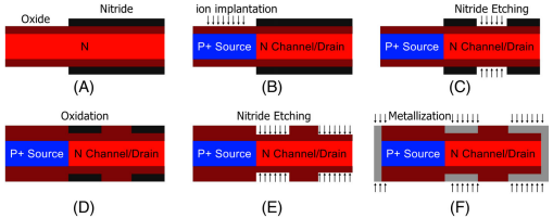
FIG: Key steps for fabrication of the proposed DEDG-TFET

Acknowledgement: This work was supported by Ministry of Electronics & Information Technology (MeitY), Government of India through Visvesvaraya PhD Scheme.

Reading about #OpenSource in French https://t.co/A5lXEvoSOL https://t.co/OjByvKO4la


from Twitter https://twitter.com/wladek60

June 05, 2020 at 10:55AM
via IFTTT

Jun 4, 2020

[paper] Large-signal behavioral model for RF power transistors

Cai J, King J, Liu J, Wang J, Sun L.
Large-signal behavioral model for radio frequency power transistors 
based on modified canonical sectionwise piecewise-linear functions
IJNM 2020;e2767
DOI: 10.1002/jnm.2767

Abstract: A novel, large-signal behavioral modeling methodology for radio frequency power transistors, based on the modified canonical sectionwise piecewiselinear (CSWPL) functions, is presented in this article. The basic theory of the proposed model is provided. Compared with the existing standard CSWPL model, the proposed model provides superior prediction capabilities for a reasonable increase in model complexity. Model verification is performed through comparisons with simulated and experimental data of a 10 W GaN HEMT device at mild and severe mismatch conditions, across a wide range of input power levels. The models can predict, more accurately, both the fundamental and the second harmonic scattered waves compared with the standard CSWPL model.
Fig: Comparison between circuit, CSWPL model, and proposed modified CSWPL model, when the available input power is 5dBm, the number of partitions K=J=3, and the number of Fourier terms L=3

Correspondence: Jialin Cai, The Key Laboratory of RF Circuit and System, Ministry of Education, Hangzhou Dianzi University, Hangzhou, CN


[paper] Unified Analytical Transregional MOSFET Model

Kalra, S, Bhattacharyya, AB. 
A Unified Analytical Transregional MOSFET Model for Nanoscale CMOS Digital Technologies
Int J Numer Model. 2020; 33:e2700
https://doi.org/10.1002/jnm.2700

Abstract: For IC designers, power has always been the main design constraint. Near threshold (moderate inversion) computing is a promising technique to manage power and energy requirements. A modeling framework specific to moderate inversion is developed in literature known as Transregional Mosfet Model (TRM). This paper presents an extension of TRM model by considering the lateral and vertical field dependent mobility of carriers that make it suitable for circuit design at supply voltages not restricted to near threshold voltage. The model proposed is the unified model applicable in all operating regions (weak, moderate, and strong) and all saturation levels from a long channel with negligible effect of velocity saturation to a short channel having extreme velocity saturation. Further, it has been shown that the proposed drain current model can be reduced to unified interpolated expression of EKV model for long channel MOSFET.

FIG: Comparison of (A) proposed model, (B) weak inversion approximation, (C) strong inversion approximation, with transregional MOSFET model (TRM) and BSIM4 at 22nm technology node. 


[paper] On-Wafer FinFET-Based EUV/eBeam Detector Arrays

Wang, Chien-Ping, Yi-Pei Tsai, Burn Jeng Lin, Zheng-Yong Liang, Po-Wen Chiu, Jiaw-Ren Shih, Chrong Jung Lin, and Ya-Chin King
On-Wafer FinFET-Based EUV/eBeam Detector Arrays for Advanced Lithography Processes
IEEE TED (2020)

Abstract: A novel microdetector array (MDA) for monitoring electron beam (eBeam) and extreme ultraviolet (EUV) lithography processes in 5 nm and beyond FinFET technology is first-time presented. This on-wafer detector array consists of high-density sensing cells which are fully compatible with standard FinFET CMOS processes. Fin coupling structures and energy-sensing pads are first applied in an ultrasmall detector for realizing efficient eBeam and EUV photon detection. In advanced lithography process, eBeam or EUV level projected on the wafer can be precisely recorded on the on-wafer MDA without power or batteries. The distributions and variations on the beam intensities collected by MDA can be electrically measured in real time or inline through wafer level test after eBeam or EUV exposures. The proposed MDA is expected to provide real-time feedback for the optimization and stable maintenance of advanced photolithography processed critical to the development nanometer CMOS technologies.
FIG: (a) Schematic of lithography system and (b) 3-D illustration of unit detector cell of the MDA consisting of ESP and FG on the shallow trench isolation (STI) region.

Acknowledgment: The authors gratefully acknowledge the contributions of Taiwan Semiconductor Manufacturing Company (TSMC) and Ministry of Science and Technology (MOST), Taiwan (Project Number: MOST 108-2622-8-007-017).